
Jagadeesh Mummana
Visakhapatnam, India
Electronics undergrad exploring chip design, robotics, and real-world ML systems. This is my little corner of the internet, where you’ll find my work, ideas, and experiences.
Education
Bachelor of Technology in Electronics and Communication Engineering
2023 - 2027 | Calicut, Kerala, India
Grade: 8.51/10 (CGPA)
Lab Involvement
Technical Member
Nov 2024 - Present
Kerala, India
Working on several real-world interdisciplinary projects as part of robotics enthusiast teams while representing the institute on competitive platforms
Summer Research Intern
May 2026 - July 2026
Odisha, India
FPGA/ASIC-Optimized RTL Automation and Comparative Hardware/Statistical Evaluation of LFSR-Derived and Cellular Automaton-Based PRPG Architectures in BIST
Summer Project Member
Apr 2025 - July 2025
Kerala, India
Trained models for MRI-based Alzheimer’s & MCI classification
Featured Projects
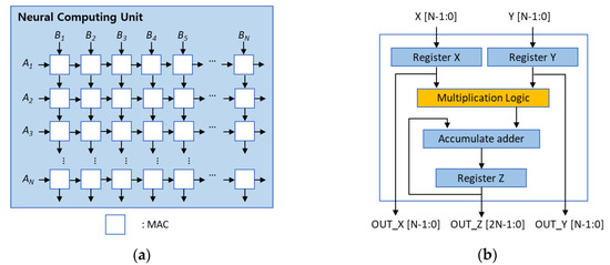
INT8 Fixed-Point CNN Hardware Accelerator and Image-Processing Suite
Designed and implemented a quantized Res-CNN with hardware acceleration, fixed-point analysis, ROM automation, and AXI-Stream image processing blocks.
View Project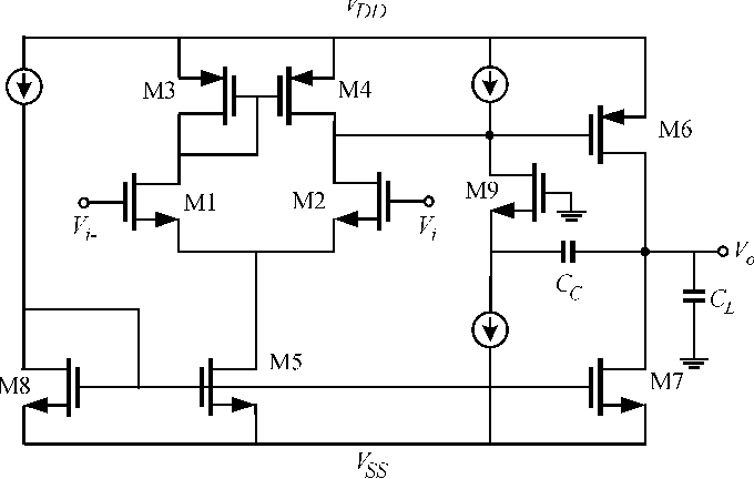
Two-Stage CMOS Op-Amp with Miller Compensation
Designed and analyzed a two-stage CMOS op-amp with Miller compensation and measured small-signal and stability metrics.
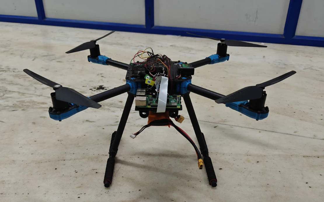
Autonomous Drone for GNSS-Denied Environments (ISRO IRoC-U 2025)
Designed and validated a quadrotor platform for GNSS-denied navigation with visual–inertial localization and simulation.
View ProjectFeatured Blogs
April 5, 2026
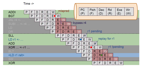
Optimising a Pipelined RISC-V Core: From Naive Pipeline to Near-Superscalar Performance
This post walks through the complete optimization journey of a single-issue pipelined RV32I core, from a plain five-stage implementation all the way to a version that runs within 2.3% of a superscalar design on CoreMark. Every number here comes from actual simulation runs on my own implementation. This is not a theoretical survey – it is what happened, step by step, with real cycle counts.
Before getting into the details, a disclaimer worth repeating throughout: modern high-performance processors like those from ARM, Intel, or Apple are not just superscalar, they are wide out-of-order superscalar with speculative execution, branch prediction trained on billions of cycles of silicon, register renaming, reorder buffers, and execution units that would make what is described here look like a toy. That context matters, and so does what this comparison intentionally excludes. All CoreMark/MHz figures here are frequency-normalized because superscalar and superpipelined designs face harder timing closure, with wider forwarding muxes, more register file ports, and longer critical paths. Collapsing everything into a single clock frequency number would obscure the microarchitectural comparison. The goal here was never to match a Cortex-A or an M-series core.

May 15, 2025
Why RISC-V Is Better for Custom Silicon

January 3, 2025
Hello World!!
Recent Blogs
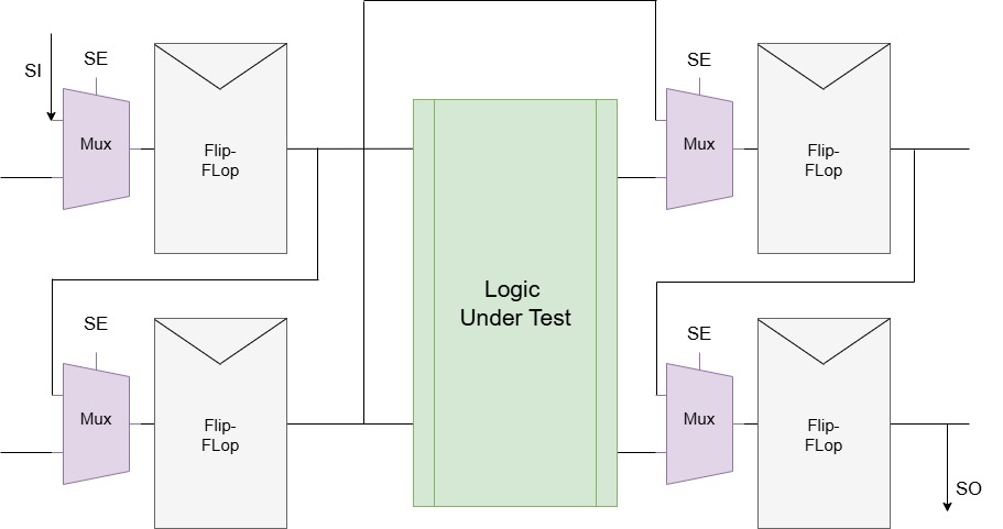 DFT Scan Insertion on a NoC Router: Working Around OpenLane 2's Missing DFT Support
Jun 6, 2026
DFT Scan Insertion on a NoC Router: Working Around OpenLane 2's Missing DFT Support
Jun 6, 2026
 Building a Hardware Scan-Line Triangle Rasterizer: From Single-Pixel Core to SIMD Warp Architecture
May 10, 2026
Building a Hardware Scan-Line Triangle Rasterizer: From Single-Pixel Core to SIMD Warp Architecture
May 10, 2026
 My First Tiny Tapeout: Building a Digital PLL on Sky130
Apr 20, 2026
Optimising a Pipelined RISC-V Core: From Naive Pipeline to Near-Superscalar Performance
Apr 5, 2026
My First Tiny Tapeout: Building a Digital PLL on Sky130
Apr 20, 2026
Optimising a Pipelined RISC-V Core: From Naive Pipeline to Near-Superscalar Performance
Apr 5, 2026