
Introduction to VLSI Design Flow: RTL to GDSII
Wonder why AI, modern smartphones, and countless digital devices have become so powerful yet compact? The secret lies in the ability to pack billions of transistors into tiny silicon chips — a feat accomplished through Very Large-Scale Integration (VLSI). At the core of this accomplishment is a complex, multi-step design flow that transforms abstract hardware concepts into a physical chip ready for fabrication.
This flow spans multiple abstraction layers, engineering disciplines, and verification cycles, culminating in a GDSII layout file — the silicon mask data sent to the foundry. The path from Register Transfer Level (RTL) to GDSII involves a series of crucial steps, each demanding specialized tools and deep expertise. Understanding this journey is essential to appreciate how high-level design intentions translate into intricate transistor arrangements and interconnected metal layers, ultimately defining chip functionality, performance, power, and reliability.
Overview of VLSI Design Flow Stages
Before diving into the details, here is a list of the core stages in the VLSI design flow, following the journey from high-level design to final chip layout:
- RTL Design
- Functional Verification
- Logic Synthesis
- Design for Testability (DFT) Insertion
- Floorplanning
- Placement
- Clock Tree Synthesis (CTS)
- Routing
- Static Timing Analysis (STA)
- Physical Verification (DRC, LVS, etc.)
- GDSII File Generation
Each stage transforms the design closer to a physical reality and imposes critical constraints for the subsequent steps. Let’s explore each of these stages with a detailed, low-level perspective.
RTL Design: Abstract Behavioral Description
At the foundation of any digital IC design lies the Register Transfer Level (RTL) description. Here, engineers use Hardware Description Languages like Verilog or VHDL to describe data flow between registers and the combinational logic applied to that data during clock cycles.
The RTL is an algorithmic, cycle-accurate model specifying how registers transfer data, how multiplexers select inputs, how finite state machines transition between states, and how arithmetic operations execute. It abstracts away transistor-level details and focuses on the logic-level function.
This abstraction allows for flexible architectural exploration — for example, deciding the number of pipeline stages or datapath widths — long before hardware resources are allocated. The RTL code forms the contract between what the chip should do and how it will later be implemented.
Functional Verification: Exhaustive Behavioral Testing
Designing a complex chip solely based on code is risky without rigorous validation. Functional verification ensures that the RTL code behaves exactly as intended, catching logical errors, corner cases, and unexpected behaviors.
Verification engineers write testbenches, which generate input stimulus and check outputs against expected results. They use simulation tools to emulate the design cycle-by-cycle, checking timing, control signals, and data correctness. Formal verification techniques and assertion-based verification (SVA) are also employed to mathematically prove design properties.
The verification scope covers both typical and edge cases, attempting to exhaustively exercise all possible scenarios. Detecting and correcting bugs at this stage prevents costly iterations in physical design.
Logic Synthesis: Mapping RTL to Gate-Level Implementation
Once the RTL passes functional verification, it enters logic synthesis — the translation of behavioral code into a gate-level netlist of standard cells.
Synthesis tools map abstract RTL constructs like if-else statements and case blocks into logic gates such as NANDs, NORs, and flip-flops from a predefined standard cell library. The process includes:
- Technology mapping: Choosing gate types optimized for the target fabrication technology node (e.g., 7nm, 14nm).
- Logic optimization: Minimizing gate count, reducing delay, and balancing power consumption.
- Constraint application: Incorporating timing goals, area budgets, and power constraints specified by the designer.
The synthesized netlist represents a logical implementation ready for physical design. However, it remains technology-dependent and not yet placed or routed on silicon.
Design for Testability (DFT) Insertion: Facilitating Post-Silicon Testing
Modern chips consist of billions of transistors, making direct transistor-level testing impractical. Therefore, Design for Testability (DFT) techniques are integrated to enable effective manufacturing tests.
Common DFT techniques include:
- Scan insertion: Flip-flops are replaced or augmented with scan cells connected into scan chains, allowing serial loading and observation of internal states.
- Built-In Self-Test (BIST): Logic to generate test patterns internally to check memory arrays or logic blocks.
- Boundary scan: For I/O pin testing using standardized protocols (IEEE 1149.1).
DFT insertion is carefully balanced against area overhead and timing impact but is essential to detect manufacturing defects and improve yield.
Floorplanning: Defining the Physical Architecture
Transitioning from logical netlists to a physical layout starts with floorplanning. This stage defines the macro-level organization of the chip:
- Silicon core size and aspect ratio
- Placement of Input/Output (I/O) pads
- Approximate locations for large blocks like memories and IP cores
- Power grid and clock domain planning
Floorplanning establishes the canvas for subsequent steps. It aims to reduce routing congestion, optimize timing, and provide sufficient space for power delivery networks. Poor floorplanning choices can cascade into routing difficulties, timing violations, and increased power consumption.
Placement: Detailed Cell Positioning
With a floorplan set, the standard cells from the netlist must be precisely placed. Placement tools assign exact coordinates for each cell to:
- Minimize interconnect wirelength, which impacts delay and power
- Reduce congestion to facilitate routing
- Optimize timing by clustering cells on critical paths
Placement algorithms consider timing slack, cell density, and power grid connections to ensure a balanced, manufacturable layout. Placement quality significantly affects the chip’s speed, power, and routability.
Clock Tree Synthesis (CTS): Distributing the Clock Signal
The clock signal synchronizes operations across the chip and must arrive at every sequential element with minimal skew and jitter. Clock Tree Synthesis (CTS) constructs a buffered network of clock drivers and buffers:
- Distributes the clock signal evenly
- Minimizes clock skew between registers
- Balances clock latency
- Reduces power consumption of clock distribution
A well-constructed clock tree is critical to meet timing constraints and avoid data corruption caused by clock uncertainties.
Routing: Connecting the Circuit
Routing completes the physical implementation by creating metal interconnections between placed cells. Routing is performed in two phases:
- Global routing: Assigns approximate routing regions to avoid congestion hotspots
- Detailed routing: Lays out exact wire paths on available metal layers
Routing must obey design rules, spacing, and layer usage constraints. It must also mitigate parasitic effects such as crosstalk and signal delay, which can impact signal integrity and timing.
Routing is often the most time-consuming step due to the sheer complexity and number of nets.
Static Timing Analysis (STA): Timing Closure Verification
Post-routing, the design undergoes Static Timing Analysis (STA) to verify all timing paths meet constraints:
- Checks setup and hold times for sequential elements
- Computes timing slack for all paths
- Detects timing violations that can cause malfunction at the target clock frequency
STA is exhaustive and deterministic, analyzing every possible timing path without requiring test vectors. Timing failures must be resolved iteratively through design changes or buffering until timing closure is achieved.
Physical Verification: Ensuring Manufacturability and Correctness
Before sending the design for fabrication, it undergoes rigorous physical verification to ensure manufacturability:
- Design Rule Checks (DRC): Verify all layout geometry complies with foundry spacing, width, and layering rules.
- Layout Versus Schematic (LVS): Ensures the physical layout matches the netlist connectivity and topology.
- Additional checks for antenna effects, electromigration, and other reliability concerns are performed.
These steps prevent costly manufacturing errors and guarantee that the chip will function as designed.
GDSII File Generation: The Final Tape-Out
The entire physical design is converted into a GDSII file, a binary format that contains detailed polygonal data representing every layer and feature of the chip layout.
This file is the definitive mask data used by the semiconductor foundry to fabricate the chip via photolithography. It encapsulates the result of months of design effort, verification, and optimization into a manufacturable format.
The GDSII is often the final output delivered to fabrication, marking the transition from design to physical silicon.
Conclusion
The VLSI design flow from RTL to GDSII is a meticulous, multi-disciplinary journey that transforms abstract digital logic into a physical silicon chip. Each step — from writing behavioral code to verifying manufacturability — involves deep technical challenges and precision engineering.
Understanding this flow is critical for anyone engaged in semiconductor design, as it reveals how a digital idea becomes a tangible, functioning integrated circuit powering today’s technology landscape.
The constant interplay between design abstraction, physical constraints, and verification rigor drives innovation and ensures chips meet ever-increasing demands for speed, power efficiency, and functionality.
Related Posts

Sensors in Robotics: How Ultrasonic, LiDAR, and IMU Work
Sensors are to robots what eyes, ears, and skin are to humans—but with far fewer limits. While we rely on just five senses, robots can be equipped with many more, sensing distances, movement, vibrations, orientation, light intensity, and even chemical properties. These sensors form the bridge between the digital intelligence of a robot and the physical world it operates in.
Read more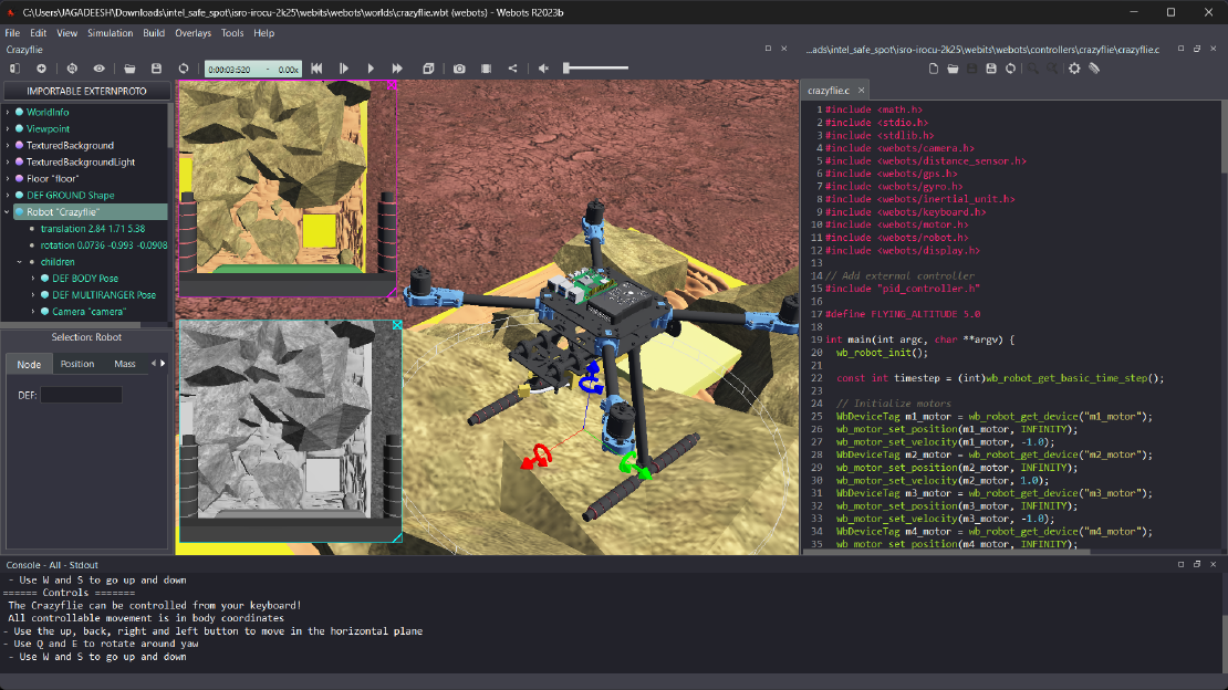
Debugging a Robot In Simulation Before You Burn Wires
Hardware does not come with an undo button. Once you power it on, mistakes—from reversed wiring to faulty code—can result in costly damage. Motors may overheat, printed circuit boards (PCBs) can be fried, and sensors may break. These issues turn exciting projects into frustrating repair sessions. The autonomous drone shown above, designed for GNSS-denied environments in webots as part of the ISRO Robotics Challenge, is a perfect example—where careful planning, testing, and hardware safety were critical at every step
Read more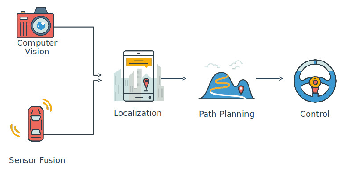
Computer Vision vs. Sensor Fusion: Who Wins the Self-Driving Car Race?
Tesla’s bold claim that “humans drive with eyes and a brain, so our cars will too” sparked one of the most polarizing debates in autonomous vehicle (AV) technology: Can vision-only systems truly compete with—or even outperform—multi-sensor fusion architectures?
Read more