Designing a Simple RTL Block for ASIC vs FPGA: A Pipelined 8-bit MAC
A Pipelined 8 Bit MAC Example
We will design a simple block defined by:
\[ Y = Y + (A \times B) \]
This is an 8 bit signed multiply accumulate unit.
You will find this block in:
- DSP filters
- CNN accelerators
- Matrix multipliers
- Control loops
The mathematical function is the same whether you build it for an ASIC or an FPGA.
The way you implement it is different.
Functional Specification
Inputs:
clkrstvalidA[7:0]B[7:0]
Output:
Y[31:0]
Behavior:
- When
validis high, computeA * B - Add the result to an internal accumulator
- Drive the updated sum on
Y
Basic RTL That Works Everywhere
module mac8 (
    input  wire        clk,
    input  wire        rst,
    input  wire        valid,
    input  wire signed [7:0] A,
    input  wire signed [7:0] B,
    output reg  signed [31:0] Y
);

reg signed [15:0] mult;

always @(posedge clk) begin
    if (rst) begin
        Y <= 0;
        mult <= 0;
    end else if (valid) begin
        mult <= A * B;
        Y <= Y + mult;
    end
end

endmodule
This is functionally correct.
It is not tuned for FPGA or ASIC.
Looking at It from an FPGA Point of View
FPGAs include:
- Dedicated DSP slices
- Block RAM
- LUT fabric
- Hard carry chains
Multipliers built from LUTs consume noticeable resources. Multipliers mapped to DSP blocks are efficient.
If synthesis sees:
mult <= A * B;
it usually infers a DSP slice automatically, provided the operand widths match what the device supports.
Match the DSP Width
For example, a Xilinx DSP48 block typically supports an 18 by 25 multiplier.
An 8 by 8 multiply maps cleanly.
If you choose unusual widths such as 13 by 13, the mapping can become inefficient and waste DSP capacity.
Add Pipelining for Higher Frequency
DSP slices have internal pipeline stages. To reach higher clock frequency, you should register inputs and intermediate values.
A better structured version:
reg signed [7:0] A_r, B_r;
reg signed [15:0] mult_r;

always @(posedge clk) begin
    if (rst) begin
        A_r <= 0;
        B_r <= 0;
        mult_r <= 0;
        Y <= 0;
    end else if (valid) begin
        A_r <= A;
        B_r <= B;
        mult_r <= A_r * B_r;
        Y <= Y + mult_r;
    end
end
Now the operation is split into stages:
- Stage 1 registers inputs
- Stage 2 performs multiplication
- Stage 3 accumulates
Shorter combinational paths allow higher clock frequency.
Keep Combinational Logic Shallow
In FPGA designs, routing delay is often larger than pure logic delay.
Several short pipeline stages are usually better than one long combinational chain.
Prefer Synchronous Reset
FPGAs generally work better with synchronous reset logic:
if (rst)
    Y <= 0;
Asynchronous resets should only be used when required.
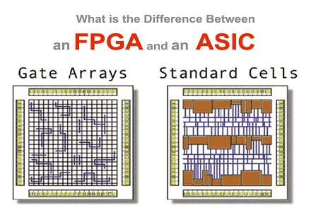
Looking at It from an ASIC Point of View
An ASIC does not have DSP slices.
Everything is built from:
- Standard cells
- Multipliers synthesized from logic
- Adders
- Registers
Multiplication consumes noticeable area and adds delay.
ASIC Oriented View of the Same Design
In an ASIC flow:
- The multiplier architecture matters.
- The critical path must be controlled.
- Area must be managed carefully.
Relying blindly on the * operator gives control to the synthesis tool.
Simple Combinational Multiplier
Let the tool infer the multiplier.
Advantages:
- Fast to write.
- Reasonable for small sizes such as 8 by 8.
Disadvantages:
- The tool may choose an implementation that uses more area than expected.
- The delay may be larger than desired.
Pipelined Multiplier and Accumulator
Breaking the multiply and accumulate into stages reduces the critical path.
reg signed [15:0] mult_stage;
reg signed [31:0] acc_stage;

always @(posedge clk) begin
    if (rst) begin
        mult_stage <= 0;
        acc_stage <= 0;
        Y <= 0;
    end else if (valid) begin
        mult_stage <= A * B;
        acc_stage <= acc_stage + mult_stage;
        Y <= acc_stage;
    end
end
Increasing pipeline depth usually improves timing at the cost of additional registers.
ASIC Specific Improvements
Booth Encoding for Larger Widths
For wider multipliers such as 16 by 16, radix 4 Booth encoding reduces the number of partial products. This lowers both delay and area.
In such cases, you may instantiate a custom multiplier macro instead of relying on *.
Control Accumulator Width
Bit growth must be considered.
\[ 8 \times 8 = 16\text{-bit} \]
If you accumulate results over many cycles, the accumulator width must be large enough to prevent overflow.
In an ASIC, every additional bit increases:
- Area
- Power
- Routing load
The width should be chosen based on actual requirements, not guesswork.
Clock Gating for Power Reduction
Power is a primary concern in ASIC design.
Instead of simply writing:
if (valid)
    Y <= Y + mult;
you can use a clock gating cell to disable the clock to the accumulator registers when valid is zero. This reduces dynamic power.
This technique is common in ASIC flows and less common in FPGA designs.
Multi Cycle Path Option
If high throughput is not required, the multiplier can be allowed to run across multiple cycles.
This reduces area but increases latency.
It is frequently used in low power ASIC designs.
Timing Closure Differences
FPGA
- Routing delay often dominates.
- Adding registers usually helps.
- DSP internal pipelines help.
- Maximum frequency depends on placement.
ASIC
- Gate delay is important.
- Wire delay becomes significant in advanced nodes.
- Cell sizing affects timing.
- Buffer insertion impacts both timing and power.
Differences in Synthesis Constraints
FPGA
Typically:
- A single clock constraint is defined.
- The tool handles placement and routing together.
ASIC
You must define:
- SDC timing constraints
- Clock uncertainty
- Input and output delays
- False paths
- Multi cycle paths
Example SDC:
create_clock -period 2.0 clk
set_input_delay 0.2 -clock clk [all_inputs]
set_output_delay 0.2 -clock clk [all_outputs]
The quality of constraints directly affects timing and area results.
Conceptual Resource Comparison
On FPGA:
- One DSP slice
- Several LUTs
- Registers
- Fixed routing fabric
On ASIC:
- Standard cell multiplier
- Adder structure
- Flip flops
- Clock tree
- Impact on floorplan and congestion
Physical Design Impact
In an ASIC:
- The placement of the MAC affects congestion.
- The accumulator fanout affects routing.
- The multiplier critical path should be physically localized.
- Placing the MAC near its data source reduces wire length.
In an FPGA:
- DSP slices are located in fixed columns.
- The design should align with available DSP placement.
- Floorplanning can improve timing.
Same RTL Different Outcomes
Case 1: Large unpipelined multiplier
On FPGA:
- Timing may fail.
On ASIC:
- The tool increases cell sizes.
- Power consumption rises.
Case 2: Deep pipeline
On FPGA:
- Higher maximum frequency is usually achieved.
On ASIC:
- More registers increase clock tree power.
- A balance must be found.
Verification Remains the Same
The testbench does not change between FPGA and ASIC targets.
Example:
initial begin
    rst = 1;
    #10 rst = 0;

    valid = 1;
    A = 8'd10;
    B = 8'd5;
    #10;

    valid = 1;
    A = -8'd3;
    B = 8'd4;
end
The functional behavior must match in both implementations.
The implementation strategy differs.
Final View
ASIC design focuses on:
- Area efficiency
- Power reduction
- Timing closure at gate level
- Awareness of physical effects
FPGA design focuses on:
- Correct DSP inference
- Proper pipelining
- Efficient resource use
- Tool friendly RTL structure
The Verilog description is only the starting point.
A practical design must consider the target technology.
When writing RTL, always check:
- Is the target FPGA or ASIC
- Is the multiplier mapping controlled
- Is the pipeline depth intentional
- Is the accumulator width justified
- Is clock power considered
Correct functionality is necessary.
Mapping the design properly onto silicon is equally important.