Analog-to-Digital Converters (ADCs): Architecture Taxonomy, Analog Front-End Realities, and System-Level Selection
Every modern electronic system is fundamentally a mixed-signal system. Sensors, RF front-ends, control loops, biomedical instrumentation, imaging systems — all begin in the analog domain. The Analog-to-Digital Converter (ADC) is the boundary where physics becomes computation.
Selecting an ADC is not a matter of “highest resolution” or “fastest sampling rate.” It is a multi-dimensional optimization problem involving:
- Dynamic range
- Signal bandwidth
- Noise floor
- Power consumption
- Latency
- Process constraints
- System architecture
This article expands beyond architectural summaries and focuses heavily on the analog realities that govern converter performance.
Sampling Theory — The Starting Constraint
An ADC does not merely convert voltage to bits. It samples a continuous-time signal.
The Nyquist criterion states:
\[ f_{signal} \leq \frac{F_s}{2} \]
Where:
- \( F_s \) is sampling frequency
- \( f_{signal} \) is maximum signal frequency
However, real systems are limited not only by sampling rate but by:
- Aperture jitter
- Input bandwidth
- Front-end settling time
- Anti-aliasing filter roll-off
Quantization — The Idealized Limit
For an ideal N-bit ADC, the quantization step is:
\[ LSB = \frac{V_{ref}}{2^N} \]
The theoretical Signal-to-Noise Ratio (SNR) for a full-scale sine input is:
\[ SNR_{ideal} = 6.02N + 1.76 , \text{dB} \]
However, practical converters never achieve ideal performance because:
- Comparator noise
- Thermal noise
- Reference noise
- Clock jitter
- Nonlinearity (INL/DNL)
All degrade real-world performance.
The effective number of bits (ENOB) is:
\[ ENOB = \frac{SNDR - 1.76}{6.02} \]
Where SNDR includes distortion and noise.
The Analog Front-End (AFE): Where Performance Is Won or Lost
Before the ADC core, the analog front-end defines system fidelity.
It typically includes:
- Input buffer or driver amplifier
- Anti-aliasing filter
- Sample-and-hold network
- Reference circuitry
Input Driver Requirements
The driver must:
- Settle within acquisition time
- Provide sufficient slew rate
- Drive capacitive load
- Maintain linearity
If the ADC sampling capacitor is \( C_s ), and acquisition time is \( T_{acq} ), then the driver must settle to within:
\[ V_{error} < \frac{1}{2} LSB \]
Settling failure directly reduces ENOB.
Clock Jitter
Clock uncertainty limits SNR for high-frequency inputs:
\[ SNR_{jitter} = -20 \log (2\pi f_{in} \sigma_t) \]
Where:
- \( f_{in} \) = input frequency
- \( \sigma_t \) = RMS clock jitter
In RF systems, jitter dominates quantization noise.
Reference Voltage Stability
ADC linearity and accuracy depend heavily on reference quality.
Key metrics:
- Temperature coefficient
- Load regulation
- PSRR
- Noise spectral density
Poor reference design often reduces precision more than ADC core limitations.
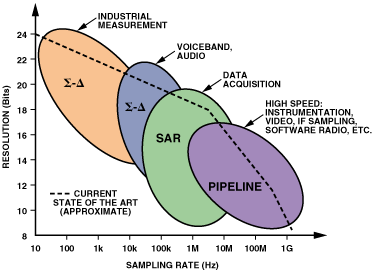
ADC Architectures
Flash ADC — Speed-Optimized Architecture
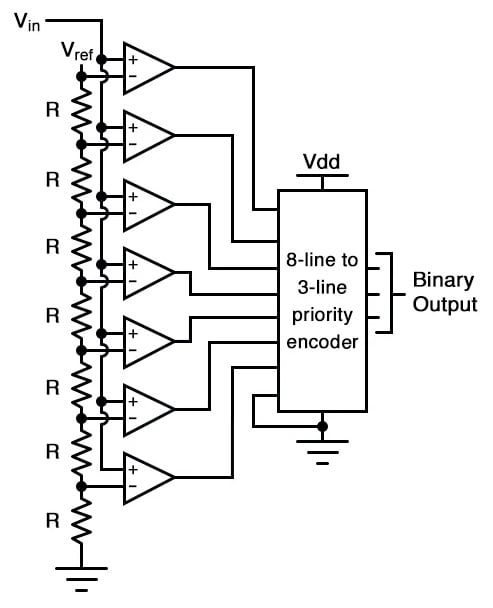
Core Principle
A flash ADC uses \( 2^N - 1 \) comparators to evaluate all thresholds simultaneously.
- Resistor ladder generates reference voltages
- Comparators create thermometer code
- Encoder converts to binary
Strengths
- Zero latency (single conversion cycle)
- Extremely high sampling rates (GHz)
- Deterministic timing
Limitations
- Exponential area scaling
- High static power
- Comparator offset mismatch
- Significant input capacitance
Analog Realities
- Comparator kickback noise affects input
- Matching of resistor ladder critical
- Offset calibration often required
Use Cases
- High-speed oscilloscopes
- RF digitizers
- Radar systems
- High-speed serial links
Flash ADCs are throughput-dominant but power-intensive.
SAR ADC — Energy-Efficient Workhorse
Core Principle
Successive Approximation Register (SAR) ADC performs binary search:
- Sample input
- Compare against DAC output
- Update bit decision
- Repeat for N cycles
Architecture Components
- Capacitive DAC array
- Comparator
- SAR logic
- Sample-and-hold
Why SAR Is Efficient
- Only one comparator
- No continuous bias current
- Scales well in CMOS
Key Analog Challenges
- Capacitor mismatch (affects INL)
- Charge redistribution noise
- Reference settling speed
- Comparator offset
Typical Operating Envelope
- Resolution: 8–18 bits
- Sampling rate: kS/s to 10 MS/s
- Low power consumption
Use Cases
- Battery-powered systems
- Industrial sensing
- Embedded control loops
- Data acquisition modules
SAR provides optimal power-performance-area balance.
Sigma-Delta (ΔΣ) ADC — Precision Through Oversampling
Core Principle
Sigma-Delta ADC oversamples input and uses noise shaping.
The modulator pushes quantization noise outside signal band:
\[ Noise_{shaped}(f) \propto f^L \]
Where \( L \) is modulator order.
Digital filtering then removes out-of-band noise.
Strengths
- Very high resolution (16–24 bits)
- Excellent dynamic range
- Relaxed analog precision requirements
Limitations
- High latency
- Complex digital filtering
- Limited bandwidth
Analog Constraints
- Loop stability
- Integrator linearity
- Reference drift
- Clock precision
Use Cases
- Audio codecs
- Precision instrumentation
- Medical devices
- Energy metering
Sigma-Delta is resolution-dominant and noise-resilient.
Pipeline ADC — Balanced Speed and Resolution

Core Principle
Pipeline ADC divides conversion into stages:
- Each stage resolves a few bits
- Residue amplified and passed forward
- Digital error correction applied
Architecture Blocks
- Sub-ADC
- Multiplying DAC (MDAC)
- Residue amplifier
- Digital correction logic
Strengths
- High throughput (tens to hundreds of MS/s)
- Moderate resolution (8–16 bits)
- Efficient for communication systems
Analog Challenges
- Residue amplifier linearity
- Inter-stage gain matching
- Op-amp bandwidth constraints
- Calibration complexity
Use Cases
- Wireless baseband
- Software-defined radio
- Imaging systems
- IF sampling
Pipeline ADCs are bandwidth-optimized with moderate precision.
Comparative Selection Matrix
| Application | Bandwidth | Resolution | Power Budget | Recommended Architecture |
|---|---|---|---|---|
| Audio | Low | High | Moderate | Sigma-Delta |
| IoT Sensor | Low | Medium | Ultra-Low | SAR |
| Oscilloscope | Very High | Low-Medium | High | Flash |
| SDR | High | Medium | Moderate | Pipeline |
| Industrial DAQ | Low-Medium | High | Moderate | SAR / Sigma-Delta |
Emerging Trends in ADC Design
- Time-interleaved ADCs for multi-GS/s
- Background calibration engines
- Digital-assisted analog correction
- Ultra-low-power (<10 µW) converters
- Machine-learning assisted calibration loops
Modern ADCs are increasingly hybrid systems combining strong digital correction with precision analog front-ends.
Final Engineering Perspective
ADC selection is fundamentally about signal integrity preservation under constraints.
It requires understanding:
- Noise sources
- Analog settling
- Clock stability
- Reference integrity
- Power budgets
- System bandwidth
There is no universally optimal ADC.
Each architecture dominates within a specific performance envelope.
Professional mixed-signal design is not about maximizing specifications — it is about aligning architecture with system requirements while controlling non-idealities.