Analog-to-Digital Converters: Architecture Taxonomy, Analog Front-End Realities, and System-Level Selection
An ADC is the interface between the physical world and computation. The choice of architecture determines not just the achievable resolution and speed, but the noise floor, the power budget, the latency, and in some cases whether the system can be made to work at all given the signal characteristics and process constraints. Understanding ADC selection means understanding the tradeoffs at each performance boundary, not just memorizing which architecture goes with which application.
This post covers the dominant ADC architectures in depth, the analog front-end constraints that govern performance before the converter core is even reached, and the quantitative tools for comparing converter quality across different types.
Sampling and Quantization: The Idealized Starting Point
An ADC performs two operations: it samples a continuous-time signal at discrete instants, and it quantizes the sampled amplitude to one of $2^N$ discrete levels.
The Nyquist criterion sets the minimum sampling rate: to reconstruct a signal with bandwidth $f_{signal}$, the sampling frequency must satisfy $f_s \geq 2f_{signal}$. This is a necessary condition, not a sufficient one. The requirement that follows from the Nyquist criterion is that all signal energy above $f_s/2$ must be removed before the sampler, because aliasing folds that energy back into the baseband and cannot be distinguished from legitimate signal content. The anti-aliasing filter design is a direct consequence of the chosen sampling rate.
For an ideal $N$-bit converter with no noise sources other than quantization, the quantization step is:
$$ \Delta = \frac{V_{ref}}{2^N} $$and the resulting quantization noise, modeled as uniformly distributed over $\pm\Delta/2$, has power $\Delta^2/12$. For a full-scale sinusoidal input, the signal-to-noise ratio is:
$$ SNR_{ideal} = 6.02N + 1.76 \text{ dB} $$This is the theoretical ceiling. Every non-ideal effect in the analog front-end, the converter core, and the reference circuit degrades SNR below this ceiling. The effective number of bits (ENOB) quantifies where a real converter actually sits:
$$ ENOB = \frac{SNDR - 1.76}{6.02} $$where SNDR (signal-to-noise-and-distortion ratio) includes both noise and harmonic distortion. An ENOB of 10 for a nominally 12-bit converter means that 2 bits of the specified resolution are consumed by noise and distortion and are not available for signal. The gap between nominal bits and ENOB is the most honest single-number characterization of converter quality in its operating condition.
The Analog Front-End
The analog front-end is everything between the signal source and the ADC’s sampling network. It is where most system-level performance is won or lost, because signal degradation at the front end is permanent: no amount of digital processing recovers information that was corrupted before sampling.
Input Driver and Settling
The ADC’s sampling network presents a dynamic load to the driving circuit. At the sampling instant, a sampling switch closes and connects the input to a sampling capacitor $C_s$. The driving circuit must charge $C_s$ to within $\Delta/2$ of the true input voltage before the switch opens and the ADC begins conversion. If the settling is incomplete, the sampled voltage is in error, which degrades ENOB directly.
The settling time requirement constrains the output impedance and slew rate of the driving amplifier. For an $N$-bit converter with sampling capacitor $C_s$ and acquisition time $t_{acq}$, the driver must settle to within $\Delta/2$ where $\Delta = V_{ref}/2^N$. A higher-resolution converter tolerates smaller absolute settling error, which requires a faster, lower-impedance driver. The driver’s noise contribution, its input common-mode range, and its distortion at the operating signal level all directly affect ENOB, often more than the converter core itself.
Clock Jitter
The sampling instant is defined by the clock edge. Any uncertainty in the timing of that edge, characterized by its RMS value $\sigma_t$, causes the sampled voltage to deviate from the ideal by approximately $\sigma_t \cdot dV/dt$ evaluated at the sampling instant. For a sinusoidal input at frequency $f_{in}$, the worst-case jitter-induced SNR is:
$$ SNR_{jitter} = -20\log(2\pi f_{in} \sigma_t) $$At low signal frequencies, jitter-induced error is small because $dV/dt$ is small even for large $\sigma_t$. As the input frequency increases, jitter becomes the dominant noise source rather than quantization noise. For a 14-bit converter sampling at 100 MSPS, the jitter limit for 14-bit ENOB at Nyquist ($f_{in} = 50$ MHz) is approximately $\sigma_t < 220$ femtoseconds. That is achievable with a careful low-noise crystal oscillator and a clock distribution network designed to minimize additive jitter, but it is not achievable with a general-purpose clock output. In RF-sampling ADCs where the input frequency is several hundred MHz or in the GHz range, jitter requirements drop into the sub-100-femtosecond range and become a system-level design challenge independent of the converter architecture.
Reference Stability
The reference voltage defines the full-scale range and sets every code boundary in the converter. Reference noise appears directly at the output: a noise voltage $v_n$ on the reference shifts every code transition by $v_n / V_{ref}$ relative to the full scale, which adds to the noise floor. Reference temperature coefficient causes gain drift with temperature. Reference load transients, caused by the converter’s sampling network drawing current from the reference during conversion, cause reference voltage perturbations that modulate the conversion result.
A high-resolution converter requires a reference with noise spectral density well below the quantization noise level, low temperature coefficient (typically under 10 ppm/°C for 16-bit applications), and a fast recovery time from load transients. In practice, the reference circuit and its decoupling network are frequently the limiting factor in achieving the ENOB that the converter core is capable of.
Flash ADC
A flash ADC resolves $N$ bits in a single conversion cycle by instantaneously comparing the input against all $2^N - 1$ threshold voltages in parallel. A resistor ladder generates equally spaced reference voltages between ground and $V_{ref}$. Each of the $2^N - 1$ comparators fires when the input exceeds its assigned threshold. The comparator outputs form a thermometer code (a string of ones followed by a string of zeros) that a priority encoder converts to binary.
The flash architecture’s single-cycle latency makes it the only choice when conversion must complete within one clock period at frequencies above a few hundred megahertz. RF digitizers in oscilloscopes and radar receivers use flash converters precisely because no other architecture matches the throughput. GHz-range sampling rates are achievable.
The cost is area and power that scale exponentially with resolution. An 8-bit flash requires 255 comparators. A 10-bit flash requires 1023. Beyond 8 bits, the input capacitance of the comparator bank becomes a significant load on the signal source, and the power consumption from 1023 continuously biased comparators becomes prohibitive. Comparator offset mismatch is another practical constraint: each comparator has a random offset voltage due to transistor mismatch, and this offset must be smaller than one LSB for the thermometer code to be monotonic. At 8-bit resolution, one LSB is $V_{ref}/256$, which is approximately 20 mV for a 5V reference. Achieving this across 255 comparators without calibration requires careful layout and sizing. In practice, 6-bit flash cores are common; 8-bit requires some form of offset correction.
The large parallel comparator bank also introduces comparator kickback, where the comparator’s internal switching transients couple back through the input and disturb the sampled voltage. Isolation between the comparator bank and the input sampling node is necessary to control this.
SAR ADC
The successive approximation register ADC performs a binary search over the input range, resolving one bit per clock cycle. The conversion sequence: close the sampling switch to acquire the input on the capacitive DAC, open the switch, compare the input against $V_{ref}/2$ (the midpoint of the full-scale range), set the MSB based on the comparator result, adjust the DAC to $3V_{ref}/4$ or $V_{ref}/4$ accordingly, compare again, set the next bit, and repeat for all $N$ bits. $N$ clock cycles produce $N$ bits.
The capacitive DAC performs two functions simultaneously: it is the sample-and-hold that captures the input voltage, and it is the DAC that generates the successive approximation voltages. The capacitors in the DAC array are binary-weighted: the MSB capacitor has value $C$, the next $C/2$, down to the LSB capacitor at $C/2^{N-1}$. Each bit decision is implemented by switching the appropriate capacitor from ground to $V_{ref}$ or vice versa, redistributing charge across the array and shifting the voltage at the comparator input.
The SAR architecture is efficient because it uses a single comparator, which can be powered down between decisions, and a capacitive DAC that consumes no static current. Dynamic power scales with sampling rate and $C \cdot V^2 \cdot f$, but there is no continuous bias path. This makes the SAR the dominant choice in energy-constrained applications: battery-powered sensors, implantable medical devices, IoT nodes. The figure of merit for SAR ADCs, measuring energy per conversion step, has improved by several orders of magnitude over the past two decades through careful sizing of the DAC capacitors and the comparator.
The resolution ceiling for SAR converters is set by capacitor matching. The DAC accuracy depends on the ratio between capacitor values, and random process variation limits how well matched those ratios can be. At 12 bits, capacitor mismatch is manageable with careful layout and unit-cell-based DAC structures. At 16 bits, mismatch calibration becomes necessary. Beyond 18 bits, the DAC settling time after each bit decision also becomes a limitation: the capacitor array must settle to within $\Delta/2$ within the allocated time for each approximation step, which becomes progressively harder as $\Delta$ shrinks.
At medium resolution (10 to 14 bits) and moderate sampling rates (up to a few tens of MSPS), the SAR offers the best energy efficiency of any ADC architecture and is the natural default for signal chain designs that do not require the extreme resolution of sigma-delta or the extreme throughput of pipeline or flash.
Sigma-Delta ADC
The sigma-delta architecture achieves high resolution through oversampling and noise shaping rather than through precision analog components. The converter samples the input at a rate much higher than Nyquist, typically by a factor of 16 to 512 depending on the target resolution, and uses a feedback modulator to spectrally shape the quantization noise so that most of it falls outside the signal band. A digital decimation filter then removes the out-of-band noise and reduces the data rate to the Nyquist rate.
The noise shaping is the key mechanism. A first-order sigma-delta modulator has a quantization noise power spectral density that rises with frequency as $f^2$ (first order) rather than being white. The noise in the signal band, which is a small fraction of the total bandwidth, is proportional to the oversampling ratio raised to the power of the modulator order. For a first-order modulator with oversampling ratio $M$:
$$ SNR \approx 6.02N + 1.76 + 30\log_{10}(M) - 5.17 \text{ dB} $$Each doubling of the oversampling ratio adds approximately 9 dB of SNR (1.5 bits). Higher-order modulators achieve steeper noise shaping and faster SNR improvement with oversampling ratio, but require stability analysis to ensure the feedback loop does not become unstable with large input signals. A second-order modulator adds approximately 15 dB per doubling of oversampling ratio; higher orders add more but introduce stability concerns that require careful design.
The consequence is that sigma-delta ADCs achieve 16 to 24 bits of resolution with analog components that are far less precise than a 16-bit SAR would require. The comparator in a sigma-delta modulator does not need to resolve 16-bit accuracy; it only needs to make a coarse decision (1-bit or a few bits), and the resolution emerges from the filtering. This relaxes the requirements on the analog circuitry at the cost of high sampling rate and complex digital filtering.
The limitation is bandwidth. Because the oversampling ratio must be high for the noise shaping to achieve high resolution, the maximum signal bandwidth is $f_s / (2M)$ where $f_s$ is the sampling rate and $M$ is the oversampling ratio. A modulator running at 10 MHz with an oversampling ratio of 256 supports a signal bandwidth of only 19.5 kHz. This is appropriate for audio (which requires 20 kHz bandwidth at 24-bit resolution) and precision instrumentation (which typically measures slowly varying signals) but is not suitable for wideband applications.
Sigma-delta is also high-latency. The decimation filter introduces a group delay proportional to the filter order and the oversampling ratio. For a sinc filter with oversampling ratio 256, the group delay is 256 input samples, which at a 10 MHz sampling rate is 25.6 microseconds. In control loop applications where latency matters, this may be unacceptable.
Pipeline ADC
A pipeline ADC partitions the $N$-bit conversion into a cascade of stages, each resolving a small number of bits (typically 1.5 to 3 bits per stage with digital error correction). The first stage resolves the most significant bits, amplifies the residue by a factor of $2^k$ (where $k$ is the number of bits resolved in that stage), and passes the amplified residue to the next stage. Each stage operates in parallel on the residue from the previous stage, so the converter achieves full throughput after an initial latency equal to the number of stages.
The residue amplifier is the central component in each pipeline stage and is typically the circuit that limits the converter’s performance. It must amplify the residue by exactly the required gain, settle within one clock cycle, and maintain linearity over the full input range. Any gain error causes a scaling error in the bits resolved by subsequent stages; any nonlinearity in the amplifier appears directly in the INL of the converter output. Achieving the required linearity at high speeds requires an op-amp with sufficient open-loop gain and bandwidth, and the power consumption of this amplifier dominates the pipeline stage’s power budget.
The 1.5-bit stage (resolving 1 bit with one redundant bit for error correction) is the dominant architecture in modern pipeline ADCs because it relaxes comparator offset requirements substantially. The comparator thresholds in a 1.5-bit stage are $\pm V_{ref}/4$ rather than $\pm V_{ref}/2^k$ for a $k$-bit stage without redundancy. This means the comparator offset can be as large as $V_{ref}/4$ and still be corrected by the digital backend, which removes the need for comparator offset cancellation in each stage and simplifies the analog design.
Pipeline ADCs target the middle ground: resolutions of 8 to 16 bits at sampling rates of tens to hundreds of MSPS. This range covers wireless baseband ADCs, cable TV receivers, digital oscilloscope front ends, and imaging sensor readout. The architecture is less energy-efficient than SAR at lower speeds and lower resolutions, and it cannot match sigma-delta resolution at low bandwidth, but in the gigasamples-per-second range at 10 to 14 bits it has historically been the dominant architecture. Sub-ADC calibration and inter-stage gain calibration are standard in modern pipeline designs, necessary to maintain 12-bit or better ENOB at high input frequencies.
Architecture Selection
The selection criteria reduce to four axes: signal bandwidth, required resolution (more precisely, required ENOB), power budget, and whether latency is a constraint.
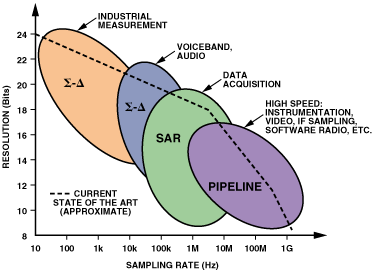
For low-bandwidth, high-resolution applications (audio, precision instruments, energy meters), sigma-delta is the only practical choice above 14 bits because no other architecture achieves that resolution without requiring analog component precision that is impossible to manufacture without tight tolerances.
For moderate bandwidth and moderate resolution (sensor interfaces, embedded control, portable instruments), SAR from 10 to 14 bits offers the best energy efficiency and is the default choice unless there is a specific reason to use something else.
For high bandwidth at moderate resolution (wireless receivers, software-defined radio, imaging), pipeline is appropriate in the tens to hundreds of MSPS range. Time-interleaved SAR has displaced pipeline in some applications at the boundary of their operating ranges, particularly at 12 bits and 100 to 500 MSPS.
For maximum throughput at coarse resolution (RF digitization, high-speed test instruments), flash up to 6 to 8 bits, or a folding-interpolating variant that extends flash range while reducing comparator count, remains the only option when conversion latency must be under one nanosecond.
| Application | Bandwidth | Resolution | Recommended Architecture |
|---|---|---|---|
| Audio codec | 20 kHz | 20-24 bits | Sigma-Delta |
| Precision instrument | DC-10 kHz | 18-24 bits | Sigma-Delta |
| IoT sensor | DC-1 kHz | 12-16 bits | SAR |
| Industrial DAQ | DC-100 kHz | 12-18 bits | SAR or Sigma-Delta |
| Embedded MCU ADC | DC-1 MHz | 10-12 bits | SAR |
| SDR baseband | 1-50 MHz | 12-16 bits | Pipeline or interleaved SAR |
| Oscilloscope front-end | 1-10 GHz | 6-10 bits | Flash or time-interleaved pipeline |
These are defaults, not rules. A specific application may have unusual constraints (ultra-low power, non-standard supply voltage, extreme temperature range) that push the selection away from the default. The selection matrix is a starting point for analysis, not a substitute for it.
The most common selection error is optimizing for resolution specification rather than ENOB in the operating condition. A converter with a 16-bit nominal resolution and an ENOB of 12 bits in the intended application is worse than a converter with a 14-bit nominal resolution and an ENOB of 13 bits. Nominal resolution is the ideal performance; ENOB is what the application sees.