
[WIP] Dissecting the ARM Silicon in the Dimensity 1080: Per-Core CPU Tests and Mali-G68 GPU Tests


[WIP] Every phone spec sheet says “octa-core ARM processor”. That phrase hides almost everything interesting: which ARM cores, arranged how, coherent through what, clocked by what, and a GPU that is a separate processor entirely. This post opens the black box. I explain what Arm’s product families are, take the MediaTek Dimensity 1080 in my Redmi Note 12 Pro 5G apart at the block level, and then measure the CPUs and the GPU separately, using only ADB from a laptop, with no root and no third party benchmark apps.
How the measurements were made
The phone and the laptop are on the same Wi-Fi. Android’s wireless debugging gives a pairing port and code; from the laptop:
adb pair 192.168.0.104:46411      # enter the 6 digit code shown on the phone
adb connect 192.168.0.104:38911    # connect port from the wireless debugging screen
adb devices                        # 192.168.0.104:38911  device
adb shell                          # interactive shell on the phone
Everything below runs through adb shell. Where the phone’s sysfs is permission locked for the shell user (thermal zone files, battery current, Mali clocks), I used the dumpsys services instead, which are readable without root on this Xiaomi build.
The CPU benchmark is a small static aarch64 C program (bench.c: one dependent integer chain workload and one NEON fused multiply-add dot product, each timed with clock_gettime, optionally pinned to a core with sched_setaffinity). It is cross compiled on the laptop and pushed over:
aarch64-linux-gnu-gcc -O3 -static bench.c -o bench
adb push bench /data/local/tmp/
adb shell chmod +x /data/local/tmp/bench
adb shell /data/local/tmp/bench 6    # pin to cpu6
adb shell /data/local/tmp/bench -1   # unpinned, scheduler chooses
The GPU test is a WebGL scene (the Khronos aquarium sample) opened in Chrome via am start, with frame timing read back from the system: adb shell dumpsys gfxinfo com.android.chrome framestats. GPU and battery temperatures come from adb shell dumpsys thermalservice.
Arm the company, and the ISA versus the core
Arm licenses intellectual property rather than selling silicon. “ARM” strictly refers to the instruction set architecture (the ISA: instructions, registers, privilege levels, memory model). “Cortex” is Arm’s own line of CPU core designs that implement that ISA. A chip vendor such as MediaTek licenses both, integrates them with its own GPU, NPU, ISP, modem and memory controller, and fabricates the result. So “ARM phone” means “runs the Arm ISA on Arm designed or licensed cores”, not “made by Arm”.
The Cortex families and the rest of the Arm IP
| Family | Role | Notes |
|---|---|---|
| Cortex-A | Application processors | Full MMU, run Linux/Android. A55, A76, A78 are v8.2-A; A510/A720 are v9-A |
| Cortex-X | Flagship performance variant of A | Highest clocks and IPC, used 1-2 per phone |
| Cortex-R | Real time and safety | Deterministic latency, optional lockstep, used in SSD controllers, basebands |
| Cortex-M | Microcontrollers | No MMU, bare metal or RTOS, M0/M3/M4/M33/M85 etc. |
| Neoverse | Server and datacenter | V/N/E series, designed for many-core coherent systems |
Around the CPU cores, the surrounding Arm IP in a phone SoC:
- Mali: the GPU. Valhall is the current mainstream architecture (G68, G78, G710 and so on).
- Ethos: NPU for on-device machine learning (the Dimensity 1080 has MediaTek’s own APU 3.0 instead, 4.5 TOPS).
- TrustZone: splits execution into secure and normal worlds, with a secure monitor; used for DRM, biometrics, key storage.
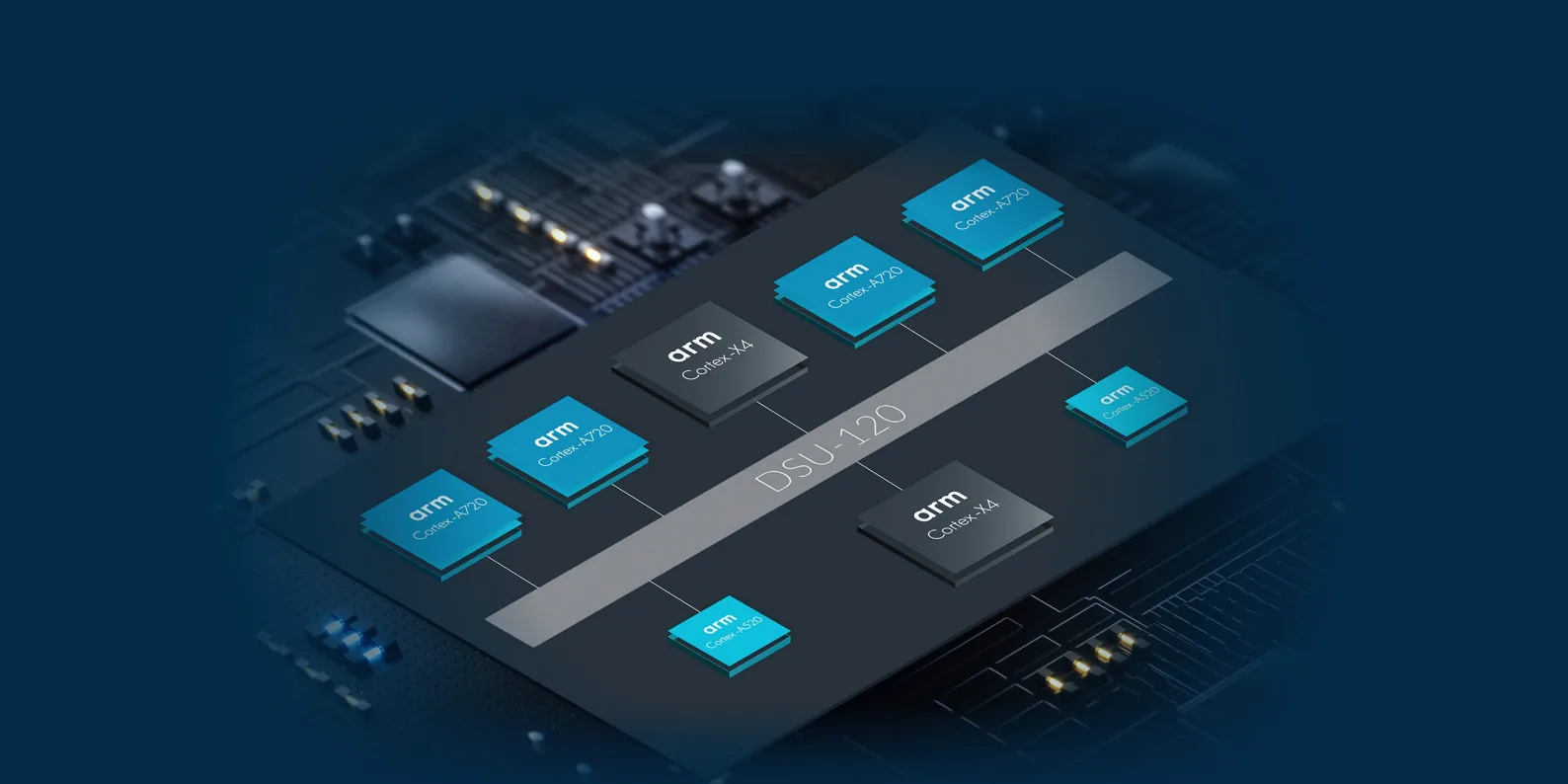
- DynamIQ Shared Unit (DSU): glues a heterogeneous cluster of up to 8 cores (max 4 big on v8.2) into one coherent domain with a shared L3.
- CoreLink CMN: the coherent mesh interconnect that links the DSU, GPU, NPU, ISP and DRAM controller inside the SoC.
The Dimensity 1080, block by block
getprop on the phone reports:
ro.soc.manufacturer = Mediatek
ro.soc.model        = MT6877V/TTZA
ro.hardware         = mt6877
That is the Dimensity 1080: TSMC 6nm, ARMv8.2-A, 64 bit. The layout that matters for this post:
                 CoreLink CMN coherent mesh
   +------------------------------------------------------+
   |   DynamIQ Shared Unit (DSU)                          |
   |   SCU + snoop filter, shared sliced L3 = 2 MB        |
   |   cpu6,cpu7 = 2x Cortex-A78 @ up to 2.6 GHz          |
   |   cpu0..cpu5 = 6x Cortex-A55 @ up to 2.0 GHz         |
   |   per-core DVFS (PPU per core), one cluster          |
   +------------------------------------------------------+
        |                     |                |
   Mali-G68 MC4 GPU      APU 3.0 NPU      LPDDR4X 2133 MHz ctrl
   950 MHz, 4 cores      4.5 TOPS         UFS 2.2, ISP, 5G modem
The two CPU types are not the same core at different clocks. The Cortex-A78 (cpu6, cpu7) is a wide out-of-order machine: 4-wide fetch and decode, a 13 stage pipeline, a 160 entry reorder buffer, a TAGE plus gshare branch predictor taking up to 2 taken branches per cycle with about a 10 cycle mispredict penalty, 64KB L1 instruction and 64KB L1 data caches, and a 512KB 8-way L2 with ECC. The Cortex-A55 (cpu0 to cpu5) is an in-order dual issue design: 2-wide decode, 32KB L1 I and 32KB L1 D, a 128KB L2, a prefetcher, and no speculative execution past an unresolved branch, so a mispredict costs little but there is also nothing to hide latency with. Both share the DSU’s 2MB L3. The DSU provides the snoop filter and SCU so all 8 cores see one coherent address space, and gives each core its own DVFS domain, which is why the two policies (policy0 for cpu0-5, policy6 for cpu6-7) scale independently.
The GPU is a Mali-G68 MC4: Valhall architecture, 4 shader cores, 128 FP32 lanes total (32 per core, each lane doing a fused multiply-add, so 256 FLOPs per clock per core), 16 texture mapping units, 8 ROPs, about 1.5MB of cache, running at 950MHz in this SoC. The theoretical FP32 peak is 128 lanes x 2 x 0.95GHz, about 580 GFLOPS. Valhall is tile based deferred rendering: geometry is binned into tiles in a first pass, then each tile is shaded using on-chip tile memory before resolve to the framebuffer, which is why it can hold 1080p 60fps scenes at low memory bandwidth.
Reading the hardware from software
/proc/cpuinfo exposes the Arm implementer ID and part number per processor:
processor 0..5 : CPU implementer 0x41, CPU part 0xd05   -> Cortex-A55
processor 6..7 : CPU implementer 0x41, CPU part 0xd41   -> Cortex-A78
The cpufreq sysfs confirms the split and the clock ceilings:
policy0 affected=[0 1 2 3 4 5]   available freqs up to 2000000 (2.0 GHz)
policy6 affected=[6 7]           available freqs up to 2600000 (2.6 GHz)
At idle the cores were at 500MHz (A55) and 1.3-1.43GHz (A78). The time_in_state counters already showed the usage pattern: cpu0 had spent 17.4M jiffies at 2.0GHz while cpu6 had real residency at 2.6GHz.
Per-core benchmark results
The integer workload is a dependent chain (each iteration depends on the previous), so it measures pipeline throughput and clock, not cache. The NEON dot product measures SIMD throughput. Results, one core at a time:
| Run | Int workload | NEON dot |
|---|---|---|
| cpu0 (A55) | 198.0 Miter/s in 0.505 s | 1.10 GMAC/s |
| cpu1 (A55) | 198.4 Miter/s in 0.504 s | 1.07 GMAC/s |
| cpu6 (A78) | 298.2 Miter/s in 0.335 s | 3.84 GMAC/s |
| cpu7 (A78) | 296.5 Miter/s in 0.337 s | 3.89 GMAC/s |
| unpinned | 299.0 Miter/s | 3.82 GMAC/s |
Two things stand out. First, the A78 is 1.50x an A55 on the integer chain even though its clock is only 1.3x higher: the extra margin is the 4-wide out-of-order backend extracting more instructions per cycle from the same dependent chain. On NEON the gap widens to about 3.5x, because the A78 sustains more SIMD work per cycle on top of the higher clock. Second, the unpinned run scored exactly like a pinned A78 run: the kernel scheduler placed the single thread on a big core by itself, which is the energy aware scheduler doing its job.
Frequency and thermal behavior under load
Sampling scaling_cur_freq every 0.5s while a loop hammered cpu6:
t=1  cpu6=910000   t=5  cpu6=2150000   t=9  cpu6=1900000
t=2  cpu6=2150000  t=6  cpu6=2150000   t=10 cpu6=2150000
t=3  cpu6=2150000  t=7  cpu6=2150000   t=11 cpu6=2150000
t=4  cpu6=1430000  t=8  cpu6=2150000   t=12 cpu6=2150000
cpu0 stayed at 500000 the whole time (one brief 2000000 sample)
The A78 ramps from 910MHz to about 2.15GHz and holds there. Note it settles below the 2.6GHz table maximum: the sustained all core boost is capped by the power and thermal management before any thermal throttle kicks in. That is the per-core DVFS doing exactly what it is designed to do.
For temperatures, the sysfs thermal zones were not readable as the shell user, but dumpsys thermalservice exposes both the live HAL readings and the throttle ladder:
CPU  hot throttling thresholds: 85.0, 90.0, 100.0, 117.0 C
GPU  hot throttling thresholds: 85.0, 90.0, 100.0, 117.0 C
BAT  hot throttling thresholds: 50.0, 55.0, 59.0, 60.0 C
During the CPU load the SoC peaked at 57.8C (CPU sensor), far below the 85C first threshold, which is consistent with the frequency trace barely moving. Battery voltage read 4114mV at 76% charge via dumpsys battery.
The GPU, measured separately
Mali’s own sysfs nodes (/sys/class/misc/mali0/device/gpuinfo, dvfs entries) were permission locked on this build, so the GPU was measured through the graphics pipeline instead of through its clock registers.
The WebGL aquarium scene was opened in Chrome with adb shell am start -a android.intent.action.VIEW -d "https://webglsamples.org/aquarium/aquarium.html". Frame timestamps from dumpsys gfxinfo com.android.chrome framestats show consecutive vsyncs 16.5ms apart:
1021197936131441 -> 1021197952656825 : 16525384 ns = 16.53 ms = 60.0 FPS
1021197952656825 -> 1021197969198009 : 16541184 ns = 16.54 ms = 60.0 FPS
... steady 16.5 ms frames across the whole window ...
So the Mali-G68 MC4 held a vsync locked 60 FPS at 1080p on this scene, with no jank visible in the frame deltas. During the same window dumpsys thermalservice showed the GPU sensor climbing from 43.3C to 49.6C and settling around 47.5-48.8C, battery at 38C, again far below the 85C GPU throttle threshold.
For an absolute reference point, UL Benchmarks’ public database lists this exact phone (Redmi Note 12 Pro, Dimensity 1080) at 2227 points in 3DMark Wild Life Unlimited with 13 FPS in graphics test 1. That is consistent with the Mali-G68 MC4’s ~580 GFLOPS FP32 theoretical peak: real scenes are limited by vertex rate, texture rate and ROPs long before the FP32 peak is reached.
The key structural point: the GPU ran this workload while the CPU cores sat near idle, because Chrome’s compositor and the WebGL driver only need a sliver of CPU. CPU benchmarks and GPU benchmarks on this phone are genuinely independent measurements of two different processors hanging off the same CMN mesh.
What this all adds up to
“Octa-core ARM phone” decodes as: two Cortex-A78 out-of-order cores plus six Cortex-A55 in-order cores in one DynamIQ cluster with a shared 2MB L3 and per-core DVFS, plus a Mali-G68 MC4 GPU on the same coherent fabric. Measured on the device itself: the A78 delivers 1.5x the integer and 3.5x the SIMD throughput of an A55 per core, the scheduler automatically lands lone threads on A78s, sustained load holds the A78 near 2.15GHz rather than the 2.6GHz burst ceiling, the SoC stays around 50-58C against an 85C throttle wall, and the GPU renders 1080p WebGL at a locked 60 FPS while warming to only about 49C. All of it was read out over wireless ADB with no root: /proc/cpuinfo for core identity, cpufreq sysfs for clocks, dumpsys thermalservice for temps and thresholds, a pushed static binary for pinned benchmarks, and dumpsys gfxinfo for GPU frame timing.
Reproduce
adb pair 192.168.0.104:46411 && adb connect 192.168.0.104:38911
adb shell 'grep -E "^(processor|CPU part)" /proc/cpuinfo'
adb shell 'for p in /sys/devices/system/cpu/cpufreq/policy*; do echo "$p: $(cat $p/affected_cpus)"; done'
aarch64-linux-gnu-gcc -O3 -static bench.c -o bench
adb push bench /data/local/tmp/ && adb shell 'chmod +x /data/local/tmp/bench'
adb shell /data/local/tmp/bench 0
adb shell /data/local/tmp/bench 6
adb shell 'dumpsys thermalservice | grep -E "mName=(CPU|GPU),"'
adb shell am start -a android.intent.action.VIEW -d "https://webglsamples.org/aquarium/aquarium.html"
adb shell 'dumpsys gfxinfo com.android.chrome framestats | tail -20'