Memory Hierarchy and Cache Mapping


A CPU can execute one instruction per nanosecond and then wait fifty nanoseconds for the data it needs. That ratio is the whole problem. Processor speed has historically improved faster than memory speed, so the gap between what the core can do and what the memory can feed it has widened every generation.
If you build a machine with no cache, the core spends most of its time completely idle, burning cycles waiting on memory. You cannot fix this by simply making main memory fast, because the memory technology that is fast enough is also far too expensive and physically large to build gigabytes of storage out of. So the standard answer is to build a small amount of fast, expensive memory close to the core and a large amount of cheap, slow memory further out, using hardware to make the small one appear to be the whole thing.
That is a cache.
I initially considered writing the cache controllers in RTL first and using simulation waveforms to back up the theory before writing this post. But writing caches is hard for where I stand right now, which is pretty evident if you look at my previous posts. It is not that the fundamental logic is impossible to wrap your head around, but the moment you try to generalize a cache design for analysis sake, debugging it turns into a huge time sink. I have not worked with multi-core or multi-level caches before, even at a high level. But I still wanted to understand how this stuff works under the hood, both for the sake of completeness for this post and of course out of my own genuine interest. So I am leaving the full multi-core RTL implementation for later and treating this as a dedicated, ground-up study of how caches, coherency, and memory consistency actually work.
The Memory Hierarchy
The memory hierarchy is a stack of storage levels, each roughly ten times larger and slower than the one above it:
| Level | Typical Size | Latency | Technology |
|---|---|---|---|
| Registers | 1 KB | Under 1 cycle | Flip-flops |
| L1 cache | 16 to 64 KB | 1 to 4 cycles | SRAM |
| L2 cache | 256 KB to 2 MB | 8 to 15 cycles | SRAM |
| L3 cache | 4 to 64 MB | 30 to 60 cycles | SRAM |
| Main memory | 8 to 64 GB | 100 to 300 cycles | DRAM |
| Storage | 512 GB to 2 TB | Millions of cycles | Flash (NVMe) or Disk |
+-----------------------------------------------------------------------------------+
|                        The Memory Hierarchy Ladder                                |
+-----------------------------------------------------------------------------------+
|  [ CPU Registers ]          < 1 KB, < 1 cycle       (Flip-flops inside pipeline)  |
|         |                                                                         |
|         v                                                                         |
|  [ Level 1 Cache (L1) ]     16 - 64 KB, 1-4 cycles  (SRAM, split I/D)             |
|         |                                                                         |
|         v                                                                         |
|  [ Level 2 Cache (L2) ]     256 KB - 2 MB, 8-15 cyc (SRAM, private/unified)       |
|         |                                                                         |
|         v                                                                         |
|  [ Level 3 Cache (L3) ]     4 - 64 MB, 30-60 cycles (SRAM, shared LLC)            |
|         |                                                                         |
|         v                                                                         |
|  [ Main Memory (DRAM) ]     8 - 64 GB, 150-300 cyc  (1T1C dynamic cells)          |
|         |                                                                         |
|         v                                                                         |
|  [ Non-Volatile Storage ]   TB, Millions of cycles  (NAND flash / SSD)            |
+-----------------------------------------------------------------------------------+
SRAM vs. DRAM: The Physics of Storage
The two silicon technologies that dictate this entire ladder are SRAM and DRAM:
- SRAM (Static RAM): Stores each bit using a six-transistor (6T) cell consisting of two cross-coupled CMOS inverters and two access transistors. Because the cross-coupled inverters form an active bistable latch, SRAM holds its data indefinitely as long as power is applied. It requires no periodic refresh cycles, and reading or writing it takes only a couple of nanoseconds. The trade-off is physical area: six transistors per bit make SRAM large on silicon, power-hungry, and extremely expensive per megabyte. That is why it is used only in small quantities right next to the processor execution units.
- DRAM (Dynamic RAM): Stores each bit as an electrical charge on a microscopic capacitor gated by a single pass transistor (a 1T1C cell). Having only one transistor per bit makes DRAM roughly six times denser and vastly cheaper to manufacture per gigabyte than SRAM. However, the capacitor is tiny (measured in femtofarads), so charge leaks away through the silicon substrate within milliseconds. DRAM controllers must constantly halt normal operations to execute periodic refresh cycles. Furthermore, reading a DRAM cell discharges the capacitor, making every read destructive: the data must be detected by sensitive analog sense amplifiers and rewritten back into the storage cells. This row activation and precharge cycle is why DRAM access latency is orders of magnitude slower than SRAM.
Every level of the hierarchy caches the level directly below it. Registers cache the L1, L1 caches the L2, L2 caches the L3, L3 caches main memory, and main memory caches non-volatile storage. The same design questions recur at each level.
Locality: Why Caching Works
A cache only works because software execution is not random. Real programs exhibit two forms of locality:
- Temporal Locality: If a processor accesses a memory address at time $t$, it is highly likely to access that same address again in the near future. Think of loop counters, stack pointers, and inner-loop instructions. Caching keeps recently touched data in fast storage so subsequent accesses hit immediately.
- Spatial Locality: If a processor accesses memory address $A$, it is highly likely to access nearby addresses ($A+1, A+2, \dots$) soon. Think of sequential instruction execution, traversing an array, or reading struct fields. Caches exploit spatial locality by transferring data not as individual bytes or words, but in fixed-size blocks (cache lines) of 16, 32, or 64 bytes. When you fetch the first byte, hardware brings the whole neighborhood along with it for free.
Almost every cache microarchitectural decision is an attempt to exploit one of these two principles.
Terminology: From Pages Down to Bytes
Hardware documentation uses a lot of overlapping terms. Walking through them in order of decreasing size helps clarify how memory is viewed:
- Virtual and Physical Addresses: A user program never touches physical DRAM pins directly. It runs in a virtual address space mapped onto physical memory frames by the operating system. This mapping is tracked in a page table stored in memory, and the base unit of mapping is a page (typically 4 KB).
- The TLB (Translation Lookaside Buffer): Walking a multi-level page table takes multiple sequential memory accesses, which would cripple performance if executed on every load or store. The virtual-to-physical translation itself is cached in a specialized structure called the Translation Lookaside Buffer. A TLB is a cache whose entries are page table translations rather than raw program data. A TLB miss triggers a hardware page table walk or a trap to operating system software.
- Blocks and Lines: A cache does not track individual bytes. It stores fixed-size chunks called blocks or lines. The terms are often used interchangeably, although strictly speaking a block refers to the raw data payload, while a line refers to the physical entry containing the data block plus its tag, valid bit, and coherency state bits. In a system with 32-byte lines, missing on a single 4-byte word causes all 32 bytes to be pulled from memory together.
- Offset, Index, and Tag: Every physical memory address presented to a cache is carved into three fields:
- Offset: The lowest bits of the address. Selects the specific byte within the cache line. For a 16-byte line, you need 4 offset bits ($2^4 = 16$).
- Index: The middle bits of the address. Selects which set (row) in the cache SRAM array to inspect.
- Tag: The remaining upper bits of the address. Stored alongside the data in the cache SRAM and compared on every access to confirm that the line currently sitting in that set is the one requested. The index does not need to be stored in the tag array because it is implicit in the physical row address of the SRAM.
- Hit and Miss: A Hit occurs when the tag stored in the cache matches the address tag and the entry’s valid bit is set. A Miss occurs when the tags do not match or the valid bit is zero, forcing the cache to stall and request the line from the next memory level.
- The Four C’s of Cache Misses:
- Compulsory Miss (Cold Miss): The very first time a program accesses a cache line. Unavoidable unless hardware prefetchers predict the access in advance.
- Capacity Miss: A miss that occurs because the cache simply is not large enough to hold all the active data working set. It would not have happened if the cache had infinite storage. The only fix is increasing cache capacity.
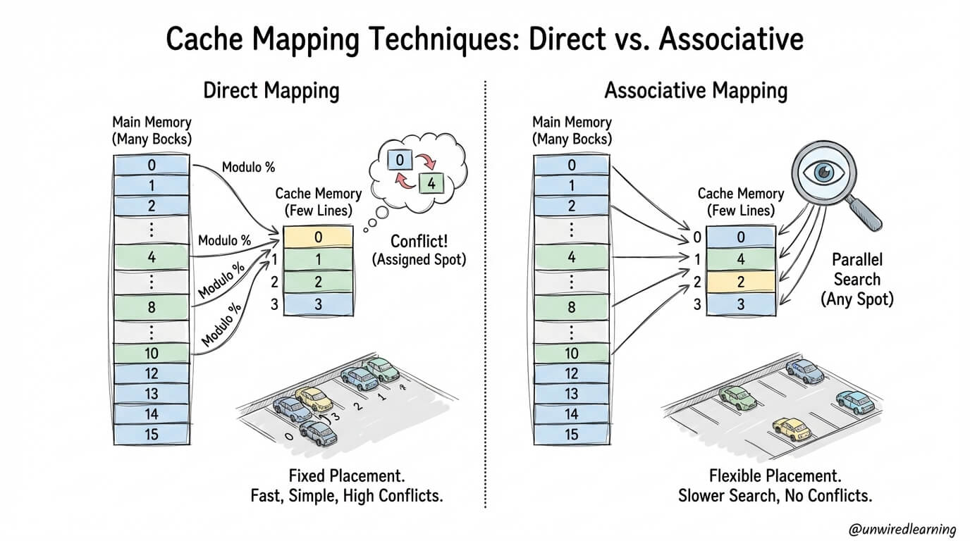
- Conflict Miss (Collision Miss): A miss that occurs because multiple active addresses map to the exact same cache set, kicking each other out even though other sets in the cache are completely empty. It would not have happened if the cache were fully associative. The fix is increasing associativity (more ways).
- Coherence Miss: Occurs in multi-core systems when another core writes to a line and invalidates your local copy.
- Average Memory Access Time (AMAT): The standard formula governing cache performance: $$ ext{AMAT} = ext{Hit Time} + ( ext{Miss Rate} imes ext{Miss Penalty})$$ Every hardware optimization targets one of these three levers: make hits faster, make misses rarer, or make misses cheaper to service.
Cache Organizations and How the Bits Actually Work
The fundamental difference between cache organizations comes down to how the index and tag fields are carved out of the memory address.
+------------------------------------+-----------------------+----------------------+
|             Tag Bits               |       Index Bits      |     Offset Bits      |
+------------------------------------+-----------------------+----------------------+
  Identifies which line is cached      Selects the set (row)   Selects byte in line
Direct-Mapped Caches
In a direct-mapped cache, each memory address maps to exactly one physical location in the cache. Each set contains exactly one line (Way count $N = 1$).
There is no replacement policy and no way-selection multiplexer. When a miss occurs, whatever line currently occupies that set is evicted immediately. This makes direct-mapped caches the fastest to read and the cheapest to build in terms of area and timing closure.
The critical drawback is conflict misses. If two frequently accessed variables happen to share the same index bits, they will evict each other on every single cycle, creating catastrophic cache thrashing even if 99% of the cache remains empty.
Direct-Mapped Address Math (4 KB Cache, 16-Byte Lines, 32-Bit Address)
Total Capacity = 4096 bytes
Line Size      = 16 bytes
Total Lines    = 4096 / 16          = 256 lines
Total Sets     = 256 / 1            = 256 sets

Offset Bits    = log2(16)           = 4 bits  (addr[3:0])
Index Bits     = log2(256)          = 8 bits  (addr[11:4])
Tag Bits       = 32 - 8 - 4         = 20 bits (addr[31:12])
Address breakdown: [ Tag: 20 bits ] [ Index: 8 bits ] [ Offset: 4 bits ]
Address: [ Tag: 20 ] [ Index: 8 ] [ Offset: 4 ]
                         |              |
                         v              |
                 Select Set (0..255)    |
                         |              |
                         v              |
                 +---------------+      |
                 | Tag   | Data  |      |
                 +-------+-------+      |
                     |       |          |
                     v       |          |
        Stored Tag == Tag?   |          |
            |                v          v
            +----------> [ MUX / Byte Select ] ---> Data to CPU
Set-Associative Caches
In an $N$-way set-associative cache, each set contains $N$ candidate lines (ways). When an address presents its index, it selects one set, and the hardware compares the incoming address tag against all $N$ tags stored in that set in parallel. If any tag matches and is valid, you have a hit. On a miss, an eviction policy picks one of the $N$ ways to replace.
Set associativity is the practical middle ground used in almost every real L1 and L2 cache. A 2-way or 4-way structure eliminates the vast majority of conflict misses while keeping tag comparison logic small and fast.
2-Way Set-Associative Address Math (4 KB Cache, 16-Byte Lines, 32-Bit Address)
Total Capacity = 4096 bytes
Line Size      = 16 bytes
Total Lines    = 4096 / 16          = 256 lines
Way Count      = 2
Total Sets     = 256 / 2            = 128 sets

Offset Bits    = log2(16)           = 4 bits  (addr[3:0])
Index Bits     = log2(128)          = 7 bits  (addr[10:4])
Tag Bits       = 32 - 7 - 4         = 21 bits (addr[31:11])
Address breakdown: [ Tag: 21 bits ] [ Index: 7 bits ] [ Offset: 4 bits ]
Notice what happened to the bit allocation: going from direct-mapped (1-way) to 2-way removed one bit from the index and shifted it into the tag. Because there are half as many sets (128 instead of 256), the index field shrunk from 8 bits to 7 bits. That freed bit had to go somewhere, so it became part of the tag. A wider tag requires an extra comparator bit, but each set can now hold two different lines that share the same lower index bits without evicting each other.
Address: [ Tag: 21 bits ] [ Index: 7 bits ] [ Offset: 4 bits ]
                 |                |
                 |                v
                 |         Select Set 0..127
                 |                |
                 v                v
         +---------------+---------------+
         |     Way 0     |     Way 1     |
         | [Tag]  [Data] | [Tag]  [Data] |
         +-------+-------+-------+-------+
                 |               |
                 v               v
            Comp == Tag?    Comp == Tag?
                 |               |
                 +-------+-------+
                         |
                         v
                Hit Logic & Way MUX
Fully Associative Caches
In a fully associative cache, there are no sets and no index bits. Every line in the cache belongs to a single giant set. An incoming address tag must be compared against the tag of every single line in the cache simultaneously.
Because an address can reside in any line in the cache, conflict misses are completely eliminated. The only misses that occur are compulsory misses and capacity misses.
Fully Associative Address Math (4 KB Cache, 16-Byte Lines, 32-Bit Address)
Total Capacity = 4096 bytes
Line Size      = 16 bytes
Total Lines    = 4096 / 16          = 256 lines
Total Sets     = 1                  (by definition)

Offset Bits    = log2(16)           = 4 bits  (addr[3:0])
Index Bits     = log2(1)            = 0 bits  (no index)
Tag Bits       = 32 - 0 - 4         = 28 bits (addr[31:4])
Address breakdown: [ Tag: 28 bits ] [ Offset: 4 bits ]
Every single address bit above the 4-bit offset belongs to the tag. A 4 KB fully associative cache with 16-byte lines requires 256 comparators running in parallel, followed by a 256-to-1 multiplexer tree to route the matching data. The capacitive wire load, power consumption, and silicon area make fully associative designs impractical for large data caches. However, for small structures like 32-entry or 64-entry Translation Lookaside Buffers (TLBs), full associativity is standard.
The Real Verilog Zero-Width Slice Bug
A subtle hardware trap arises when writing a generalized parameterized cache in Verilog. If you write:
localparam INDEX_WIDTH = $clog2(NUM_SETS);
wire [INDEX_WIDTH-1:0] index = address[OFFSET_WIDTH + INDEX_WIDTH - 1 : OFFSET_WIDTH];
For a fully associative cache, NUM_SETS is 1, so INDEX_WIDTH evaluates to 0. A zero-width part-select (address[OFFSET_WIDTH - 1 : OFFSET_WIDTH]) is illegal in Verilog and fails compilation.
The tempting quick fix is to clamp the index width to a minimum of 1 bit:
localparam INDEX_WIDTH = (NUM_SETS == 1) ? 1 : $clog2(NUM_SETS);
This compiles cleanly, but introduces a critical silent bug. Forcing a 1-bit index means address[OFFSET_WIDTH] is treated as an index rather than as part of the tag. When two addresses differ only in that bit, they are treated as having the same tag. The cache evaluates a false hit on data that was never loaded, silently corrupting execution.
The correct hardware implementation keeps the logical index width at 0 for tag arithmetic and tag comparison, using a dummy clamp strictly for the wire declaration while discarding the slice output when associativity is full.
Comparison Across Organizations (4 KB Capacity, 16-Byte Lines)
| Organization | Sets | Ways | Index Bits | Tag Bits | Comparators Required | Conflict Miss Behavior |
|---|---|---|---|---|---|---|
| Direct-Mapped | 256 | 1 | 8 | 20 | 1 | High risk of thrashing |
| 2-Way Associative | 128 | 2 | 7 | 21 | 2 | Removes majority of conflicts |
| 4-Way Associative | 64 | 4 | 6 | 22 | 4 | Diminishing conflict reduction |
| 8-Way Associative | 32 | 8 | 5 | 23 | 8 | Near fully associative hit rate |
| Fully Associative | 1 | 256 | 0 | 28 | 256 | Zero conflict misses |
Reading down the table reveals the exact engineering tradeoff: every doubling of ways cuts the number of sets in half, shrinks the index by 1 bit, lengthens the tag by 1 bit, doubles the number of comparators, and progressively eliminates conflict misses.
Other Microarchitectural Cache Decisions
Beyond associativity and sizing, several structural policies dictate cache behavior:
- Split vs. Unified: L1 caches are almost always split into separate Instruction (I-cache) and Data (D-cache) arrays. This allows the processor pipeline to fetch an instruction and perform a load or store in the exact same cycle without causing a structural hazard on a single memory port. Higher levels (L2 and L3) are unified because latency is already multi-cycle and sharing the capacity dynamically between code and data yields better hit rates.
- Blocking vs. Non-Blocking (MSHRs): A blocking cache can handle only one memory miss at a time. When a miss occurs, the cache stalls the entire pipeline until the refill data returns from main memory. A non-blocking cache (lockup-free cache) continues serving cache hits to younger instructions while an older miss is in flight. It tracks pending misses using Miss Status Holding Registers (MSHRs), enabling hit-under-miss and miss-under-miss memory pipelining. Building a blocking cache is simple, which is why baseline hardware models often carry an
m1designation (meaning exactly 1 MSHR). Non-blocking caches require complex dependency tracking and scoreboarding to prevent out-of-order data hazards. - Write-Through vs. Write-Back:
- Write-Through: Every store instruction updates the cache line and is immediately propagated to the next memory level. Memory is always kept clean and coherent, but write bandwidth demand on the interconnect is high.
- Write-Back: Stores update only the local cache line and set a Dirty Bit. The modified data is written out to lower memory only when that line is eventually evicted. Write-back caches dramatically reduce memory bus traffic.
- Write-Allocate vs. No-Write-Allocate:
- Write-Allocate: On a store miss, hardware fetches the missing line from lower memory into the cache, and then performs the write. Typically paired with write-back caches so subsequent writes hit locally.
- No-Write-Allocate: On a store miss, the data bypasses the cache entirely and modifies lower memory directly. Typically paired with write-through caches.
- Replacement Policies: When a set is full, hardware must pick a victim way to evict:
- True LRU (Least Recently Used): Tracks the exact order of access across all ways. Requires maintaining state bits that grow quadratically with way count ($N(N-1)/2$ bits), making it impractical for 8-way or 16-way caches.
- Pseudo-LRU (Tree-PLRU): Arranges the ways as leaves in a binary decision tree using $N-1$ state bits per set. Every access flips the branch bits pointing away from the accessed way. On eviction, hardware simply traverses down the pointers to locate the least recently touched candidate.
- Saturating Age Counters: Uses 1 or 2 age bits per way that increment periodically and reset on an access. Lines with saturated age counters are selected for eviction.
Multi-Core Systems: The Cache Coherency Problem
When multiple CPU cores share a memory space, each core requires private L1 caches to maintain low access latency. However, private caches introduce the coherency dilemma:
[ Core 0 ] writes 0x1000 = 42          [ Core 1 ] reads 0x1000
    |                                      |
    v                                      v
[ L1 Cache: 0x1000 = 42 ]              [ L1 Cache: 0x1000 = 0 (STALE!) ]
    |                                      |
    +-------------------+------------------+
                        |
                        v
              [ Main Memory: 0x1000 = 0 ]
If Core 0 and Core 1 both read address 0x1000, both store a local copy. When Core 0 modifies 0x1000 to 42 in its private write-back cache, Core 1’s copy becomes stale. If Core 1 reads 0x1000, it reads 0, unaware of Core 0’s write.
Coherency vs. Consistency
It is essential to separate coherency from consistency:
- Cache Coherency is strictly about a single memory address. It ensures that writes to address $X$ are observed in the same serial order by all cores, and that no core reads stale data indefinitely.
- Memory Consistency defines the rules governing the ordering of reads and writes across multiple different memory addresses ($X$ and $Y$).
Snooping vs. Directory Networks
Hardware maintains cache coherency through two architectural models:
- Broadcast Snooping: All caches connect to a shared bus. Every cache controller continuously monitors (“snoops”) the bus for addresses requested by peer cores. When Core 0 writes to address $X$, it broadcasts an invalidation across the bus, and all peer caches invalidate their copies. Snooping is low-latency for 2 to 8 cores, but because broadcast traffic grows quadratically ($O(N^2)$), it saturates the interconnect on larger systems.
- Directory-Based Coherency: Replaces broadcast buses with point-to-point networks (such as 2D meshes or NoCs). A centralized or distributed directory tracks which cores hold copies of each cache line using a bitmask. Invalidation messages are unicast directly to the specific cores holding the line, scaling to dozens or hundreds of cores.
Coherency Protocols: MSI, MESI, MOESI, and MESIF
Cache coherency protocols are implemented as state machines embedded within cache controllers.
Baseline MSI Protocol
Every cache line tracks one of three states:
- Modified (M): Valid, dirty, private to this cache. Sole owner.
- Shared (S): Valid, clean, present in one or more caches. Read-only.
- Invalid (I): Contains no valid data.
Bus transactions include BusRd (read without intent to write), BusRdX (read with intent to modify and invalidate peers), BusUpgr (upgrade shared line to modified), and Flush (supply line to bus or write back to DRAM).
The core weakness of MSI is that reading private data places it in Shared. When the core later writes to that private line, it must broadcast a BusUpgr across the bus, wasting interconnect bandwidth even though no other core holds a copy.
The MESI Protocol (Adding Exclusive State)
MESI solves this by adding the Exclusive (E) state:
- Exclusive (E): Valid, clean, and private to this cache.
When a core reads a line on a cold miss, other caches indicate via a shared bus wire whether they hold a copy. If no other cache holds the line, it enters Exclusive.
If the core subsequently writes to that line, it transitions from E to Modified (M) silently, generating zero bus transactions. Because the line was already guaranteed to be private, no peer caches need invalidation.
MESI Transition Matrix
| Current State | Local CPU Event | Bus Message | Next State | Notes |
|---|---|---|---|---|
| I | CPU Read | BusRd | E (private) / S (shared) | Fetches line from memory or cache |
| I | CPU Write | BusRdX | M | Fetches line, invalidates peers |
| S | CPU Read | None | S | Fast cache hit |
| S | CPU Write | BusUpgr | M | Invalidates peer copies |
| E | CPU Read | None | E | Fast cache hit |
| E | CPU Write | None (Silent!) | M | Zero bus traffic |
| M | CPU Read / Write | None | M | Fast cache hit |
| Current State | Bus Snoop Event | Action | Next State |
|---|---|---|---|
| S | Snoop BusRd | None | S |
| S | Snoop BusRdX / BusUpgr | Invalidate local copy | I |
| E | Snoop BusRd | Assert shared signal | S |
| E | Snoop BusRdX | Invalidate local copy | I |
| M | Snoop BusRd | Intercept, supply data, write back | S |
| M | Snoop BusRdX | Intercept, supply data, write back | I |
MOESI (Owner State) and MESIF (Forward State)
- MOESI (AMD Style): In standard MESI, when a core holding a dirty line in
Modifiedsnoops aBusRd, it must write the dirty data all the way back to main memory. MOESI introduces the Owner (O) state (dirty and shared). The owner cache supplies data directly to the requesting core over the on-chip interconnect without touching DRAM, avoiding hundreds of cycles of writeback latency. - MESIF (Intel Style): When many cores hold a clean line in
Sharedand a new core requests it, having all cores respond would flood the bus. MESIF designates exactly one cache to hold the Forward (F) state. Only the cache inFresponds to snoop read requests. TheFstate migrates to the most recent reader.
False Sharing at the Cache Line Boundary
Because caches transfer memory in 64-byte lines rather than individual 4-byte words, multi-threaded programs can suffer from false sharing.
False sharing occurs when two threads running on different cores modify independent variables that happen to reside within the same physical 64-byte cache line:
+-------------------------------------------------------------------+
|               64-Byte Cache Line at Address 0x2000                |
+---------------------------------+---------------------------------+
|   thread0_counter (4 bytes)     |    thread1_counter (4 bytes)    |
|   Accessed exclusively by Core 0|    Accessed exclusively by Core 1|
+---------------------------------+---------------------------------+
The Ping-Pong Invalidation Storm
When Core 0 writes to thread0_counter, the coherency protocol transitions Core 0’s cache line to Modified and invalidates Core 1’s copy. Next, Core 1 writes to thread1_counter. Because its local copy is now Invalid, Core 1 must issue a BusRdX over the interconnect, pulling the line into its own cache in Modified and invalidating Core 0. When Core 0 writes to thread0_counter again, it suffers an immediate cache miss, invalidating Core 1 and pulling the line right back.
The two threads never touch each other’s data, but because they share a physical cache line, the line constantly ping-pongs across the interconnect. A loop that should execute in under 1 nanosecond can slow down to 50 nanoseconds per iteration.
Software resolves this by enforcing 64-byte alignment:
// Bad: both counters share one 64-byte cache line
struct BadCounters {
    uint64_t core0_count;
    uint64_t core1_count;
};

// Good: alignas guarantees each counter starts on its own cache line
struct CleanCounters {
    alignas(64) uint64_t core0_count;
    alignas(64) uint64_t core1_count;
};
Hardware Memory Consistency Models
Cache coherency ensures all cores agree on updates to a single address $X$. Memory consistency defines the rules for how updates to different addresses ($X$ and $Y$) become visible.
Microarchitectural Reordering: Store Buffers
To maximize execution throughput, processors decouple execution pipelines from memory using Store Buffers (FIFO):
[ Execution Pipeline ] ---> Writes ---> [ Store Buffer ] ---> [ L1 Data Cache ]
         ^                                                          |
         |                                                          v
      Reads <------------------ Forwarding ------------------- Snoop Network
When a core executes a store, waiting 30 cycles for the cache line to become Modified would stall the pipeline. The core writes the data into a local Store Buffer and immediately continues executing younger instructions. The store buffer drains into the L1 cache in the background.
Store buffers boost single-thread performance, but allow younger loads to execute before older stores have drained to cache, introducing Store-Load reordering ($S_1 o L_2$).
Total Store Order (TSO - x86) and Dekker’s Failure
The x86 architecture implements Total Store Order (TSO), which guarantees all program orders except Store-Load reordering.
Consider two addresses, $X$ and $Y$, initialized to 0:
Core 0 (Thread 0)             Core 1 (Thread 1)
-----------------             -----------------
X = 1;                        Y = 1;
r1 = Y;                       r2 = X;
Under Sequential Consistency, at least one core must observe the write of the other. The outcome $r1 = 0 ext{ and } r2 = 0$ is impossible.
Under x86 TSO, however, = 0$ and = 0$ is a normal, observable outcome. First, Core 0 writes into its local store buffer while Core 1 writes into its local store buffer. Next, Core 0 executes . Because address $ is not in Core 0's store buffer, it reads directly from cache, returning . At the same time, Core 1 executes . Address $ is not in Core 1’s store buffer, so it also reads directly from cache, returning . Only afterward do both store buffers drain to cache, updating = 1$ and = 1$. Both threads observed the other thread’s store after their own load, violating Sequential Consistency.
Relaxed Consistency and Memory Fences (ARM and RISC-V)
Architectures like ARM and RISC-V allow hardware to reorder loads and stores freely as long as true data dependencies are respected.
To restore deterministic ordering when synchronizing threads, software inserts Memory Fence / Barrier instructions (fence in RISC-V, dmb in ARM, mfence in x86). When a core executes a memory fence, the execution pipeline stalls younger memory operations, drains the entire Store Buffer into L1 cache to force all pending stores to become globally visible, and flushes all pending invalidations in its Invalidation Queue. Only after every previous memory transaction has committed globally does the pipeline resume executing instructions beyond the fence.
Thread 0 (Producer)           Thread 1 (Consumer)
-------------------           -------------------
data = 42;                    while (flag == 0);
FENCE_STORE_STORE;            FENCE_LOAD_LOAD;
flag = 1;                     local_data = data; // Guaranteed 42!
Closing Thoughts
This is still far from a complete picture of how modern processors actually handle memory. Real production silicon has layers of aggressive stream and stride prefetchers, non-blocking MSHR pipelines, speculative memory disambiguation, and complex directory topologies that go far beyond basic state transitions. This post is just my fair idea of how the memory hierarchy hangs together based on what I have studied so far, and honestly, this is not my comfort zone. Execution pipelines and ALU datapaths feel much more tangible to me than multi-level cache hierarchies and memory consistency models. But getting these fundamentals straight was a necessary step, even if turning any of it into working hardware is something I will leave for later.
References
- Hennessy, J. L., & Patterson, D. A. (2017). Computer Architecture: A Quantitative Approach (6th ed.). Morgan Kaufmann.
- RISC-V International. The RISC-V Instruction Set Manual, Volume I: Unprivileged Architecture.