
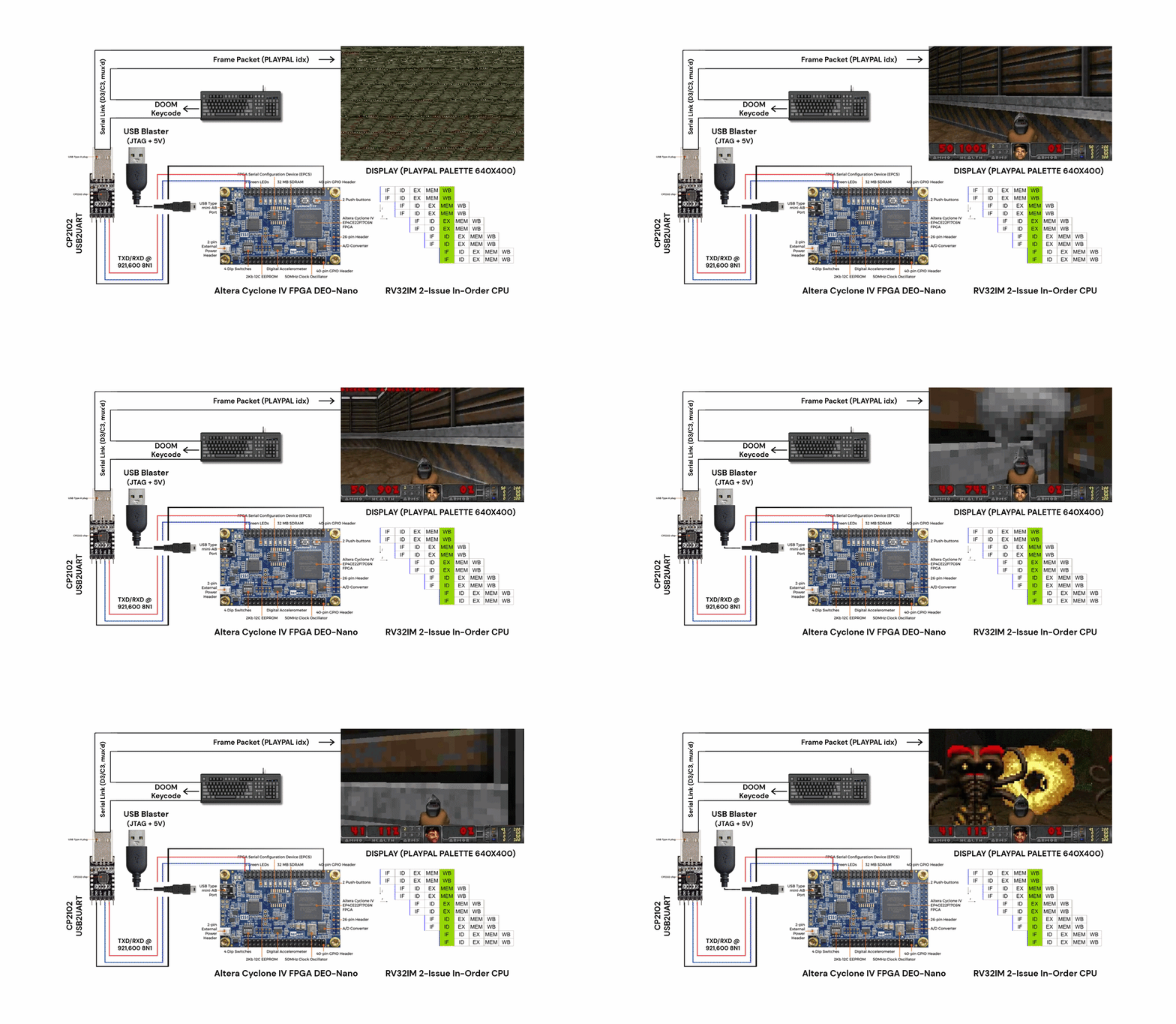
DOOM on Bare-Metal FPGA


The core was validated in Verilator with a dual issue in order RV32IM pipeline, a hybrid predictor, a BTB, and a return address stack. A DOOM gameplay workload ran for more than 500 million instructions at a CPI of 0.727 in that simulation. I then moved the design to a Terasic DE0-Nano, where the FPGA implementation added practical constraints around arithmetic, predictor storage, SDRAM latency, serial bandwidth, and the physical board wiring.
The board: a Terasic DE0-Nano
The bench starts with the board, and this post means one specific board, not FPGAs in general: a Terasic DE0-Nano, the e-Yantra lab-in-a-box kit documented on their Cyclone IV page, which ships the board and a USB cable and not much else. The silicon at its center is an Altera Cyclone IV E, part number EP4CE22F17C6N, speed grade 6, in a 256-pin FineLine BGA. The device resources that mattered for this build were 22,320 logic elements, 66 M9K embedded RAM blocks, 66 18x18 multipliers, and up to 153 user I/O pins. The later FPGA build had to stay within those logic, memory, and I/O limits.
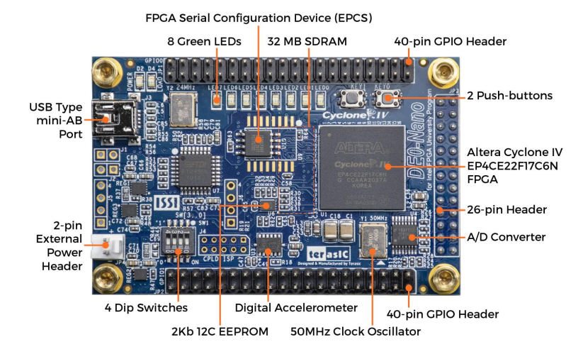
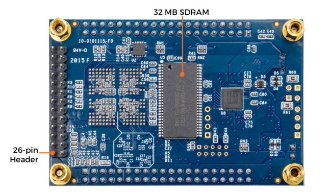
Around the die, the parts used by this project included 32 MB of SDRAM on a 16 bit bus. The game code, WAD image, heap, and framebuffer all had to fit within that memory. The board also provides a 50 MHz oscillator and an on-board USB-Blaster. The Mini-USB connection powers the board and provides JTAG programming.
The board also provides two debounced pushbuttons, eight green LEDs, and a four-position DIP switch. In this project, the LEDs showed the heartbeat, serial activity, and tester status.
The rest of the board went unused: the ADXL345 accelerometer, the 8-channel 12-bit ADC, the 2 Kb EEPROM, the 64 Mb configuration flash. Bitstreams here loaded volatile over JTAG and were never flashed, so none of those parts were touched.
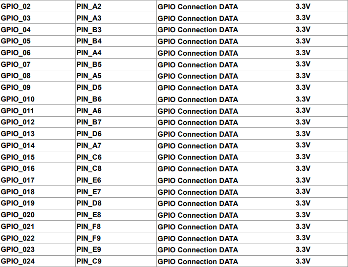
Expansion is two 40-pin headers, GPIO-0 (JP1) and GPIO-1, carrying 72 user I/O between them plus 5V, two 3.3V pins, and four grounds. This project wires GPIO-0 only; GPIO-1 sits empty, which is why it gets the overview figure and no detail table.
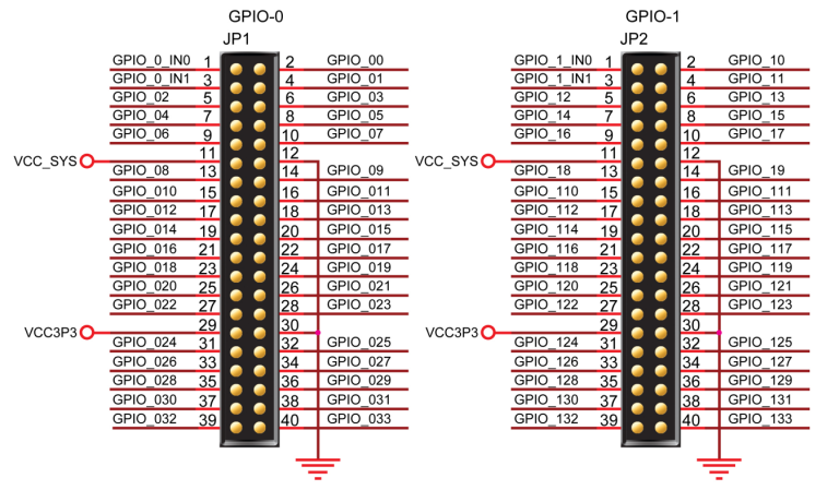
Of GPIO-0’s forty pins the project touches three. Pin 2 (FPGA pin D3) takes the serial module’s transmit line, pin 4 (FPGA pin C3) returns receive, and pin 12 is ground; pins 11 and 29 carry 5V and 3.3V for daughter cards and nothing here draws from them. Numbering runs odd down one row and even down the other, as shown in the figure. The pin table also needed one clarification: pin 40 is GPIO, while pins 12 and 30 are grounds. This build used pin 12 as the shared ground for the serial module.
The toolchain
Yosys was still useful for quick synthesis runs and for seeing which parts of the design were taking up space. I had hoped to use an open-source flow for the whole build, but the Cyclone IV support I found stopped short of a complete Verilog-to-bitstream flow. I checked nextpnr and the small EP4CE6 bitstream project too, but neither was something I could use for this board. I ended up using Quartus Prime Lite for synthesis and fitting, TimeQuest for timing, and Quartus Programmer to load the bitstream.
The annoying part was that Quartus had to run on Windows 11. Most of my setup was already on Linux SSD with other tools like OpenLane, ROS, and Vivado and Vitis, and I did not want to disturb that environment for one board by installing Quartus again. I kept the Linux setup and put Quartus on Windows, so the project ended up split between the two systems. It was not ideal, but it was the route that got the DE0-Nano build running.
The first board setup task was getting the USB-Blaster driver working.
Quartus Programmer initially showed No Hardware, and Device Manager
flagged the USB-Blaster. Pointing the wizard at the driver folder
shipped with Quartus 20.1 returned Error 39 for an unverifiable
signature. The package used a 2009 kernel driver, which current
Windows integrity policy did not accept. I started Windows once with
driver signature enforcement disabled and installed it. Quartus
Programmer then showed USB-Blaster [USB-0], Auto Detect found the
EP4CE22, and the programming path was ready.
With that in place, I started with a small bring-up design rather than the CPU. It divided the 50 MHz clock to a 1 Hz LED heartbeat, echoed bytes over UART, and ran an SDRAM test. This gave me a way to check the board, clock, serial link, USB-Blaster, and memory before adding the larger DOOM design.
The wire: a CP2102 USB to TTL module
The second piece of hardware is a USB to TTL serial module built on the Silicon Labs CP2102: USB 2.0 full speed on one side, 3.3 volt logic level UART on the other, appearing on the laptop as an ordinary COM port. Its role grew through the project until it carried everything off chip: bootloader handshake and game upload, console text, framebuffer frames on the way down, keystrokes on the way up. There is no VGA, no Ethernet, no SD card: display, console, and keyboard all pass through this module, multiplexed onto two signal wires.
Only three of its pins ever connect: TXD, RXD, and ground, crossed to JP1 pins 2 and 4 with ground on pin 12, exactly as the Phase 1 wiring shows. Each side feeds itself, so the module’s power pins stay unconnected, and the 3.3 volt logic meets the FPGA banks directly with no level shifting anywhere.
One table in its datasheet went unread until Phase 2 forced the issue: the baud table. It is enough to say here that the module sets the ceiling the whole link lives under. That number comes up later, when the terminal filled with garbage and forced the issue.
Connections
+-------------------------------------------------------------------------------+
|                               DE0-Nano Board                                  |
|                                                                               |
|   +---------------------+                           +---------------------+   |
|   |   USB-Blaster JTAG  |                           |   ISSI IS42S16160   |   |
|   |  (Config + Power)   |                           |     32 MB SDRAM     |   |
|   +----------+----------+                           +----------+----------+   |
|              |                                                 | 16-bit bus   |
|              v                                                 v              |
|   +-----------------------------------------------------------------------+   |
|   |                      Altera Cyclone IV E EP4CE22                      |   |
|   |                                                                       |   |
|   |   +------------------------+             +------------------------+   |   |
|   |   |  Dual-Issue RV32IM CPU |             |  SDRAM Memory Arbiter  |   |   |
|   |   |  (50 MHz Gated Clock)  | <=========> |  & 1K-word I-Cache     |   |   |
|   |   +------------------------+             +-----------+------------+   |   |
|   |                                                      |                |   |
|   |                                                      v                |   |
|   |                                          +------------------------+   |   |
|   |                                          | UART TX/RX Controller  |   |   |
|   |                                          | & Framebuffer Streamer |   |   |
|   |                                          +-----------+------------+   |   |
|   +------------------------------------------------------|----------------+   |
|                                                          |                    |
+----------------------------------------------------------|--------------------+
                                                           |
                                                           v
                                                 +-------------------+
                                                 |   Silicon Labs    |
                                                 |   CP2102 USB-TTL  |
                                                 +---------+---------+
                                                           |
                                                           v
                                              Laptop Interactive Display
                                              (640x400 Canvas @ COM7)
Results up front
- Altera Cyclone IV E EP4CE22F17C6 (22,320 logic elements, 66 M9K
blocks, 66 18x18 multipliers), 50 MHz single clock domain, glitch
free gating through
altclkctrl. - Fit: 17,423 logic elements (78 percent) and 6,984 flip-flops, down from 29,143 nodes and 23,644 flops that overflowed the device; 54 M9K segments, 12 DSP blocks.
- IS42S16160 32 MB SDRAM on a 16 bit bus, 4.65 MB game image uploaded in 53 seconds at 921,600 baud with CRC32 verification.
- The core renders at about 35.7 frames per second internally; the serial wire delivers 160x100 at 5.75 and 320x200 at 1.44.
Phase 1: power, clock, and an echo
The bench was a DE0-Nano, a CP2102 USB to serial module, and a Windows 11 laptop, with two USB cables live at once: Mini-USB to the Nano for power and JTAG, a second cable to the serial module, both through an external hub to keep both connections available during reconfiguration. Three wires joined the boards with power off:
| Module pin | JP1 pin (GPIO-0) | FPGA pin | Purpose |
|---|---|---|---|
| TXD | 2 | D3 | Serial into the FPGA (module TX, FPGA RX) |
| RXD | 4 | C3 | Serial out of the FPGA (FPGA TX, module RX) |
| GND | 12 | Board ground | Shared reference |
The module power pins stayed unconnected.
With the programming path ready, the Phase 1 design was deliberately
small: the 50 MHz clock divided to a 1 Hz heartbeat on LED0, a UART
echo at 115,200 baud, and an SDRAM tester walking patterns across the
four banks. The serial link itself ran on a pair of
already proven UART modules, uart_rx and uart_tx:
parametrized 8N1 blocks with a clean clock/reset/data
interface, verified in loopback simulation before the board
arrived, and the same two files Phase 2 reuses with new
parameters. The echo is a
handful of registers; a received byte parks in echo_data until the
transmitter goes idle:
always @(posedge clk) begin
    if (rst) begin
        echo_pend <= 1'b0;
        tx_valid  <= 1'b0;
        tx_data   <= 8'd0;
        echo_data <= 8'd0;
    end else begin
        tx_valid <= 1'b0;
        if (rx_valid) begin
            echo_data <= rx_data;
            echo_pend <= 1'b1;
        end
        if (echo_pend && !tx_busy) begin
            tx_data   <= echo_data;
            tx_valid  <= 1'b1;
            echo_pend <= 1'b0;
        end
    end
end
The same design had passed the simulation checks, including UART
loopback at 115,200 and 2 Mbaud with zero errors and the full SDRAM
suite against a behavioral IS42S16160 model. On the board, programming
the .sof took seconds. LED0 blinked at 1 Hz, the tester finished in
about 50 ms with the expected status indications, and PuTTY on COM7 at
115,200 8N1 echoed typed characters while the activity LEDs flashed.
Together, these checks covered the board clock, JTAG programming,
serial link, and SDRAM.
Phase 2: connecting the core and fitting the FPGA
Before the fitting story, the exact CPU being fitted. This is the downscaled FPGA variant; the simulation numbers follow in brackets where they differ:
- RV32IM only: 32-bit instructions, PC advances 4 at a time, no compressed, atomic, or fence instructions.
- Dual-issue in-order core, two slots (slot 0 and slot 1), five pipeline stages: IF, ID, EX, MEM, WB.
- One ALU and one branch comparator per slot, with full forwarding that includes MEM-stage forwarding for loads and CSR reads.
- No load-use stall; the only pipeline stalls are the M-unit busy stall and the one-cycle CSR read settle stall.
- Tournament branch predictor: PC-indexed local, PC-xor-history global, and chooser tables of 2-bit counters, 16 entries each (256 in simulation), 8-bit global history, one prediction per fetch pair on slot 0.
- 16-entry branch target buffer (256 in simulation) with valid bits and full 32-bit tags and targets, plus a 16-deep return address stack.
- Branch resolution in EX for both slots with a single-cycle registered redirect.
- Multiply and divide: MUL single cycle on the DSP blocks; MULH, MULHSU, MULHU, DIV, DIVU, REM, and REMU iterative at 33 cycles each, one unit per slot inside each ALU.
- Register file: 32 registers of 32 bits, 4 async read ports, 2 clocked write ports, x0 hardwired zero on both reads and writes.
- Control and status registers: a 16-entry file indexed by the low 4 address bits, synchronous read, CSRRW/CSRRS/CSRRC operations.
- System calls and stops:
ecalland halt retire through writeback to output signals; no interrupt inputs and no privilege modes. - Clocking: a single 50 MHz domain; the core clock is the
system clock gated through
altclkctrl, frozen during SDRAM waits and stalls. - Instruction fetch: 1,024-word direct-mapped I-cache in true dual-port M9K, one port per slot, 2-cycle hits.
- Data: no data cache; two data ports share the SDRAM arbiter at about 15 cycles a transaction.
- Measured in simulation on the full core: CPI 0.727 over 500 million-plus instructions of real DOOM; the FPGA diet adds about two percent in cycles; steady state about two million cycles per frame.
Phase 2 connects the core to the SDRAM hierarchy inside
mem_top_fpga.v: a 1,024 word direct mapped I-cache in dual port
M9K with both fetch slots looking up in parallel, 2 cycle hits, an
arbiter for data at about 15 cycles a transaction, the framebuffer
mapped to the top 64 KB, the MMIO registers at the offsets the port
already uses, and a bootloader that owns the SDRAM until the PC
finishes the upload. The core runs on a clock gated through an
altclkctrl cell so the pipe pauses cleanly on SDRAM latency:
`ifdef FPGA_SYNTH
    altclkctrl #(
        .clock_type("Global Clock"),
        .ena_register_mode("falling edge"),
        .intended_device_family("Cyclone IV E"),
        .lpm_type("altclkctrl")
    ) core_clk_buf (
        .inclk(sys_clk),
        .ena(core_run_d),
        .outclk(core_clk)
    );
`else
    reg core_run_q;
    always @(negedge sys_clk) core_run_q <= core_run_d;
    assign core_clk = sys_clk & core_run_q;
`endif
The first compile failed in elaboration. Quartus refused the ID/EX
stage registers with Error 10200 and Error 12152, pointing at
if (rst || flush_ex) under
always @(posedge clk or posedge rst). Verilator compiles that into
sequential C++ without error, but synthesis must map the block
to a flip-flop with a single async clear pin, and flush_ex has no
edge in the sensitivity list, so the tool inferred latches and failed. Separating reset from flush into branches with identical
values produced a clean async clear plus a synchronous mux, zero
latches, and the benches confirmed cycle identical behavior.
With elaboration passing, quartus_map ran over 17
minutes with the host pegged before the fitter refused: 29,143
combinational nodes against 22,320 on the device. A Yosys pass over
the submodules ranked the consumers, and two structures dominated
the area, both invisible in simulation where a * b is one host
instruction and tables are free arrays:
| Module / Block | Combinational Nodes | Estimated LEs | Share of Design |
|---|---|---|---|
core_top logic (predictors, forwarding forest, ALU muxes) | 22,359 | ~12,100 | 42% |
mem_top_fpga (SDRAM arbiter, bootloader, cache ctrl) | 14,643 | ~8,000 | 27% |
registers (4-read, 2-write asynchronous register file) | 6,144 | ~3,300 | 11% |
csr_reg (Control and Status Register file) | 4,080 | ~2,200 | 8% |
Core arithmetic (muldiv, SDRAM controller, UARTs) | N/A | ~3,500 | 12% |
Each ALU carried three 64 bit multipliers and four 32 bit
dividers, doubled across the two issue slots, and the predictor
carried three 256 entry tables plus a 256 entry BTB with full tags
and targets, written as async read flop arrays costing about 19.5K
registers in core_top alone.
Arithmetic was trimmed first. MUL-low, the op the integer heavy
render loops depend on, stays single cycle combinational on the
embedded multiplier blocks. The seven wide ops moved into muldiv.v,
an iterative unit per EX slot, whose header comment describes the
protocol:
// Protocol (self-starting, no start port):
//   IDLE: if alu_op is one of the seven M ops, latch a/b and run.
//   RUN:  32 iterations, md_busy high. If alu_op stops being an M op
//         (the pipe flushed ID/EX to a bubble), abort back to IDLE.
//   DONE: md_busy low, result valid combinationally for one cycle. The
//         next state is always IDLE; a back-to-back M op starts from
//         there with the core still holding ID/EX, so no operand gap.
// The core freezes IF/ID/ID/EX/PC while md_busy is high and feeds bubbles
// to EX/MEM, so nothing samples the unit's outputs mid-run.
Shift and add multiply, non-restoring divide on magnitudes with
sign fixup, 33 cycles an op. The render math that motivated keeping
MUL fast is FixedMul, the fixed point scale used by the
column renderer, and the measured cost of the trimming on the full
game is about two percent in cycles. Proof came from vectors plus
suite: gen_md_vectors.py covers the corners (division by zero,
INT_MIN over -1, unsigned wrap) and micro_gen.py emits assembly
tests M1 through M7, writeback and forwarding, loops and calls
across divides, producer capture, chaining, signed corners, the
intra pair M dependency, every one checked to exact register values
by check_micro.py.
Even trimmed, the next compile still overflowed, registers
stuck near 19.5K in core_top. The Yosys model of core_top with
full tables showed 19,623 registers, matching Quartus within 0.3
percent. That match identified the cause: the fitter was
synthesizing the
full 256 entry predictor and PRED_SMALL was having no effect. The
QSF held one combined macro line, and Quartus 20.1 takes only the
first token of a VERILOG_MACRO string and silently drops the rest,
so the clock buffer showed the first macro active while
the predictor stayed at simulation scale:
set_global_assignment -name VERILOG_MACRO "FPGA_SYNTH=1 PRED_SMALL=1"
Splitting the line in two fixed it. Full design registers fell from 23,644 to 6,984, logic to 17,423 elements, and compile time from 17 minutes to 70 seconds:
set_global_assignment -name VERILOG_MACRO "FPGA_SYNTH=1"
set_global_assignment -name VERILOG_MACRO "PRED_SMALL=1"
One synthesis note still needed attention before moving on: Info
17036, nine MSB address nodes removed from the I-cache RAM.
inst_addr0 and inst_addr1 were declared and wired into
mem_top_fpga but never driven in doom_top, so Quartus grounded
them and every fetch would have hit address zero on silicon.
Simulation never caught it because the testbench wrapper carried
the assigns missing from the FPGA top:
assign inst_addr0 = pc_out;
assign inst_addr1 = pc_out + 32'd4;
To state it plainly: the full simulation core never fit this device. What runs on the board is the downscaled variant, with 16-entry predictor tables in place of 256-entry ones and an iterative M unit in place of wide combinational arithmetic, fitting in 17,423 logic elements where the original needed 29,143 nodes. The game runs identically on it; only the area changed.
Timing: a 34 nanosecond path in a 20 nanosecond cycle
Fitting the device is only half the job; the design still has
to meet timing. The first TimeQuest pass reported core clock
worst slack -14.5 ns, but the constraint itself was broken: warnings
332174 and 332049 showed the generated clock pattern matching zero
pins, leaving core_clk effectively unconstrained. A Tcl walk of
the post fit netlist found three clock buffers, the input, the
reset synchronizer, and the gated core clock five levels deep, and
since one star matches one hierarchy level, only the full path
resolves:
create_clock -name sys_clk -period 20.000 [get_ports CLOCK_50]
derive_clock_uncertainty

create_generated_clock -name core_clk -source [get_ports CLOCK_50] \
    -divide_by 1 [get_pins {mem|core_clk_buf|auto_generated|clkctrl1|outclk}]
With the SDC corrected, sys_clk passed clean at about +6.5 and
+6.9 ns across corners while core_clk stayed at -14.5 ns, now a
real number with total negative slack -19,379 ns.
The top failing paths all showed the same structure: EX and control registers into the PC and fetch: an async CSR read feeding forwarding muxes feeding the ALU branch compare feeding redirect and target muxes into the PC, about 34.5 ns of logic in a 20 ns cycle. The CSR file went synchronous first. The old async read mux sat on the worst path in the design, so the registered port below is the only read left, settling a cycle after the address, with the pipeline holding EX one extra cycle on CSR ops:
// CSR file with a REGISTERED read port.
//
// Timing: the old async read mux sat on the worst path in the design
// (id_ex_csr -> ... -> pc, ~35 ns). Only rdata_q exists now: it settles a
// cycle after the address is presented, and the pipeline holds EX for one
// extra cycle on CSR ops (csr_stall in core_top) so the value is always
// correct when consumed.
module csr_reg (
    input         clk,
    input         rst,
    input         we,
    input  [11:0] addr,
    input  [31:0] wdata,
    input  [2:0]  funct3,
    input  [31:0] rs1_data,
    output reg [31:0] rdata_q
);
Then branch resolution moved from ID to EX for both slots behind a registered redirect, sampled exactly once on the pair’s exit cycle:
// Both slots resolve control in EX; the redirect takes effect a cycle
// later through exr_valid/exr_pc, and the flush is extended by the same
// cycle (see flush_id/flush_ex below). Capture is blocked while EX is
// held so a resolving pair is sampled exactly once, on its exit cycle.
wire ex_redirect = ex_redirect0 || ex_redirect1;
wire [31:0] ex_redirect_pc = ex_redirect0 ? ex_actual_pc0 : ex_actual_pc1;

always @(posedge clk or posedge rst) begin
    if (rst) begin
        exr_valid <= 1'b0;
        exr_pc    <= 32'b0;
    end else if (!pipe_halt && !md_stall && !csr_stall) begin
        exr_valid <= ex_redirect;
        exr_pc    <= ex_redirect_pc;
    end
end
That move had two benefits. The backwards EX to ID forward vanished with it, and with nothing consuming forwarded data in ID anymore, the classic load-use stall fell out of the hazard unit altogether. The unit’s own comment describes the core that remained:
// NOTE: there is no load-use stall in this core. Slot-0 control resolves
// in EX (not ID), so nothing consumes forwarded data in ID anymore and
// every producer, ALU, load (via MEM forward), CSR (via MEM forward),
// is visible to EX consumers in time without stalling. The only stalls
// left are md_stall (M-unit) and csr_stall (CSR read settle), both of
// which freeze the whole front end (IF/ID/EX) directly in core_top.
Worst slack improved from -14.5 ns to -3.998 ns on the slow 1200mV, 85C corner. I also traced the remaining TimeQuest paths through the post-fit netlist instead of treating the slack value in isolation. The top paths ran from EX and control registers through the registered CSR read and forwarding muxes, into the branch comparator, redirect and target muxes, and finally the PC and fetch path. This matched the roughly 34.5 ns path seen in the initial report.
The system clock passed with about 6.5 to 6.9 ns of positive slack, and hold, recovery, removal, and pulse-width checks passed across the reported corners. The remaining setup issue was on the gated core clock at the slow corner, where total negative slack was reported as about -19,379 ns. The board was tested at nominal room conditions and the design operated there. Timing closure across all specified corners remains a separate task.
The frame 0 hang
With the retimed core the game booted, printed its headers,
rendered frame 0, and hung. A Python cycle tracer sampling the pipe
every edge plus a full SDRAM dump at the hang pointed at
the cause: the game
timestamp lasttime read -4,203 ms where the reference read 134.
The tic computation produced nonsense and the game never
got past the frame 0 wipe.
Tracing back from the corrupted timestamp led to
DG_GetTicksMs, a load into a multiply-high into a shift,
the exact sequence the game runs to turn cycle counts into
milliseconds. The tracer showed the mechanism: the load and the
mulhu issued as a pair, the dependency squashed slot 1 for
replay, and on the same edge an older M op released. The old flush
term cleared ID/EX and discarded slot 0 while the replay PC only
re-fetched slot 1, so the consumer read a stale register and the
timestamp came out corrupted:
// before: release flushes even across a squash, dropping slot 0
assign flush_ex = hz_flush_ex || md_release;
The replacement qualifies the release with the squash, so ID/EX advances slot 0 in exactly that case while redirect flushes still win:
// NOTE (squash/release fix): ID/EX must still ADVANCE slot 0 when a
// squash coincides with md_release. Flushing here drops the slot-0
// instr (it never executes and the replay PC only re-fetches slot 1),
// so its rd goes stale for the consumer. Redirect flushes still win.
wire flush_ex_idex = hz_flush_ex || exr_valid || (md_release && !squash_s1);
The regression test that captures this coincidence is nine instructions. A divide stalls the pipe, a load plus add pair arrives as the next pair and squashes at the release edge, and the test demands the load survive with exact values:
elif which=='M15':  # squash@release REGRESSION: divu stalls, Q=(lw,add) squashes at release; lw must survive
    dmem=[0]*2048; dmem[0x100]=1000
    prog=li(5,100)+li(6,7)+li(27,0x400)+[nop()]       # idx0-3 (pad: divu must be even)
    prog+=[divu(7,5,6),nop()]                          # idx4-5: M1 pair (divu slot0)
    prog+=[lw(8,27,0),add(9,8,6)]                      # idx7-8: Q pair, squashes at release
    prog+=[ecall()]                                    # idx9
    emit(prog,[(7,14),(8,1000),(9,1007)])
Tellingly, the pre fix core fails it with the exact drop signature, x8 reading 0 for 1000 and x9 reading 7 for 1007. The hazard predated the retiming and went unnoticed in simulation by timing luck; DOOM just happened to be the program that lined up the coincidence. After the change the game runs ten frames end to end at a steady two million cycles a frame, frame 0 pixel identical to the reference still, the full instruction suite matching the reference 46 for 46 with identical halts, and all six C programs halting identically. Heap level memory comparison answered the last question the long runs raised: 156 words differed, and every one traced to thinker state pointers and a small time skew between the runs, with the state records themselves byte identical and the fixed run simply further ahead in tick AI, which means the game was advancing normally rather than the core misbehaving.
The handoff that failed on six ports
The retimed core had to move from the verification tree to the Windows Quartus tree, and the first attempt moved one file. Quartus reported six Error 12002s, one per new port the retiming batch had added:
Error (12002): Port "csr_stall" does not exist in macrofunction "hz"
Error (12002): Port "rdata_q" does not exist in macrofunction "csr_file"
plus s0_ex_redirect, s0_id_csr_any, s0_id_csr_read, and
s1_id_csr_any. The receiving tree predated the batch: the new
core_top was talking to an old hazard and an old csr_reg.
Those ports are the new signals the retiming added: the redirect
out of EX, the CSR settle handshake, the registered read:
module hazard (
    ...
    input         s0_ex_redirect,
    ...
    input         s0_id_csr_read,
    input         s0_id_csr_any,
    input         s1_id_csr_any,
    ...
    input         csr_stall,
    ...
From then on the 12 core files plus defines.v moved as one atomic
package, never a single file. Compilation resumed with zero errors
at about 16K logic cells, 54 RAM segments, and 12 DSP blocks, and
the timing report read exactly as expected from the retiming
chapter: system clock passing, core clock short on the slow
corners, hold clean everywhere. The bitstream was programmed
into the board.
The board that answered in garbage
Programming succeeded, but the uploader got no reply. The
PC side looked fine: pyserial installed, COM7 present, both
files on disk, and info reporting a clean layout:
ELF: doom\doom.elf
  load @0x00000000 len  0xa626c (664.6 KB)
WAD: doom\freedoom1.wad (27.46 MB) -> @0x00d26270
total upload 28.11 MB, ~147 s at 2000000 baud
layout OK: everything inside 64 MB, clear of the fb reserve
But upload got no answer to its handshake:
COM7 @ 2000000: waiting for bootloader (HELLO)...
no bootloader answer (is the bitstream running?)
Two symptoms mattered. LEDs 0 and 1 were blinking in turn, heartbeat plus transmit activity, which on this top means the bootloader is running and sending its unsolicited ready beacon every second. And a raw terminal at 2 Mbaud showed this, repeating:
--- transcript (type to tap keys, Ctrl-C quits) ---
P¶�Z�P¶�Z�P¶�Z�P¶�Z�P¶�Z�P¶�Z�P¶�Z�
A repeating roughly six byte pattern where BLRDY1, six
bytes, belongs. The FPGA was running and transmitting; the
bytes were corrupted between the pin and the PC. That split the fault in half: not the
bitstream, not the wiring continuity, but the sampling itself, baud
accuracy or signal integrity at 2 Mbaud.
Attention turned to the adapter next. Device Manager named it a classic CP2102, VID 10C4 and PID EA60, and the datasheet gave the answer: the part divides an internal 48 MHz clock with a hard ceiling of 921,600 baud. Asking Windows for 2 Mbaud aliased to an unsupported divider, so the two ends never agreed on a bit period and every byte framed wrong. The original 2 Mbaud plan had been written against the assumption that the module could do it, and it could not.
Both ends retuned to 921,600. The receiver is parametrized oversampling, each bit sampled at its middle after a two flop synchronizer:
module uart_rx #(
    parameter CLK_FREQ = 50_000_000,
    parameter BAUD     = 115_200,
    parameter OVR      = 16,                    // oversampling ratio
    parameter DIVT     = CLK_FREQ / BAUD / OVR  // clocks per tick
) (
With oversample 6 the ideal divider is 50,000,000 over 921,600 times 6, about 9.042, so integer 9 gives exactly 54 system clocks per bit:
$$Divider = \frac{50,000,000}{921,600 \times 6} = \frac{50,000,000}{5,529,600} \approx 9.042$$$$ClocksPerBit = 9 \times 6 = 54\ system\ cycles$$$$Synthesized = \frac{50,000,000}{54} \approx 925,926\ baud$$That sits 0.47 percent above nominal, and the CP2102 side synthesizes $48,000,000 / 52 \approx 923,077\ baud$, so the ends disagree by 0.31 percent, inside the usual 2 percent budget for 8N1. The transmitter needed no new logic; it uses the same 54 clocks per bit from its own divisor. One recompile later the terminal showed clean text: HELLO answered by BLRDY1, the six bytes landing in order:
3'd0: begin   // BLRDY1
    send_len = 3'd6;
    case (b_sidx)
        3'd0: send_byte = "B";
        3'd1: send_byte = "L";
        3'd2: send_byte = "R";
        3'd3: send_byte = "D";
        3'd4: send_byte = "Y";
        default: send_byte = "1";
    endcase
end
Ten bytes of header
The handshake finally green, the next upload printed its banner and froze. The progress bar never drew a single block; within two seconds the script gave up on the very first chunk:
lost ack at offset 0
Failing at offset zero means the transfer did not degrade, it never started, and the natural suspect is the bootloader itself, crashed or wedged on the first bytes. But the bootloader had just answered the handshake, and the handshake exercises the same receive path, the same FIFO, the same transmitter the dots would use. So the receive path worked. What, then, was the FPGA waiting for?
Reading the two sides against each other showed the cause. The bootloader emits its dot per 4,096 payload bytes retired into SDRAM, counted on write acknowledges as words land in memory:
b_cnt   <= b_cnt - 32'd4;
b_total <= b_total + 32'd4;
...
end else if (((b_total + 32'd4) & 32'h00000FFF)
        == 32'd0) begin
    b_msg <= 3'd1; b_sidx <= 3'd0;   // dot
    b_send_next <= B_DATA;
    b_state <= B_SEND;
end
The host, though, counted wire bytes. It packed headers and payload into one blob, cut it into 4,096 byte slices, and demanded a dot per slice. The blob opens with a 10 byte segment header, a 2 byte count plus address and length, so the first slice carried 10 bytes of framing and only 4,086 bytes of payload. The counter sat at 4,086 against a 4,096 threshold, the dot never fired, and the host sat waiting for an acknowledgement the hardware was not scheduled to send, holding back the very next slice that contained the missing 10 bytes. A deadlock on chunk zero, and every boundary after it would have skewed the same way, since headers never touch the counter at all.
The uploader as it stands today keeps framing and payload on separate tracks. Headers go out as their own writes, and the loop measures only payload against the dot interval, asking for the dot exactly where the hardware sends it:
ser.write(struct.pack('<H', len(loads)))
all_segs = list(loads) + [(wad_addr, wad_pad)]
for addr, data in all_segs:
    ser.write(struct.pack('<II', addr, len(data)))
    data_off = 0
    while data_off < len(data):
        rem_to_dot = ACK_EVERY - (sent_payload % ACK_EVERY)
        chunk_size = min(len(data) - data_off, rem_to_dot)
        ser.write(data[data_off:data_off + chunk_size])
        data_off += chunk_size
        sent_payload += chunk_size
        if sent_payload % ACK_EVERY == 0:
            ack = ser.read(1)
            if ack != b'.':
                raise SystemExit(f'lost ack at payload offset {sent_payload} (got {ack!r})')
The same pass also hardened the handshake: the input buffer is flushed before every HELLO, so a stale beacon from the previous second can never be mistaken for an answer to this one:
for _ in range(30):
    ser.reset_input_buffer()
    ser.write(b'HELLO')
    if ser.read(6) == b'BLRDY1':
        break
With the boundaries lined up the dots streamed and the progress bar ran for the first time. It ran all the way through the executable, reached the WAD image, and halted on three new letters: RNG.
That failure was more frustrating, because the layout checker
had passed this exact image. info had printed layout OK
back when nothing worked, and the overflow checker had approved
an image the hardware now refused.
The two sides disagreed about the size of memory. The checker
measures against 64 MB, a window inherited from the simulation
data memory:
SDRAM_BYTES = 64 * 1024 * 1024
FB_RESERVE_LO = SDRAM_BYTES - 64 * 1024   # top 64 KB holds the framebuffer
while the hardware guard measures against the 32 MB device on the board, word aligned and clear of the framebuffer reserve:
wire [32:0] b_end33 = {1'b0, b_addr_r} + {1'b0, b_len};
wire b_range_ok = (b_addr_r[1:0] == 2'b0) && (b_len[1:0] == 2'b0)
    && (b_end33 <= 33'h02000000)
    && !(b_addr_r < FB_BYTE_TOP && b_end33[31:0] > FB_BYTE_LO);
The Freedoom image loads at 0x00d26270 and runs 28.8 MB, ending
at 0x0289C528, about 42.6 MB, roughly 9 MB past the IS42S16160,
four banks of four million 16 bit words. The
checker saw 42.6 inside 64 and approved; the guard saw it past 32
and aborted. Both computations were correct; they just assumed
different memory sizes.
Swapping to the shareware doom1.wad (4,196,020 bytes, MD5
f0cefca49926d00903cf57551d901abe) brought the whole package, ELF
at zero, WAD blob at _wad_start, heap above, framebuffer in the
top 64 KB, to 4.65 MB. The full upload takes 53 seconds at 921,600
baud with the CRC echoing OK, leaving about 27 MB of heap headroom,
and the uploader can now exit entirely: a no-term flag
exits after the CRC match instead of opening the terminal, freeing
COM7 for the viewer that takes the port next. DOOM booted
into E1M1
with console tics streaming over the wire.
Video over a serial wire
Running but headless: the game alive, progress visible only as tic lines scrolling past. A VGA DAC board would have solved that in an afternoon, but no DAC was on the desk, and the serial wire already on the bench was the obvious candidate. DOOM renders into a contiguous 64 KB buffer of palette indices. What if the frames just came down the wire?
The first thing to work out was what 64,000 bytes at 92,160 bytes a second does to a game loop. The answer is 0.7 seconds per frame, and the question underneath is what the game sees during those 0.7 seconds. DOOM reads time from its tick counter, and the tick counter is the cycle counter divided by a thousand. Let the core run while the UART drains and every frame injects two dozen phantom tics between renders: physics advancing in large steps, controls sampled with stale timing, monster thinkers skipping animation frames. The frames would arrive but the game logic would break.
So the frame commit freezes the game clock for the transfer.
When the engine writes MM_DUMP, the memory system drops the
core clock
enable, and the game clock divides the gated cycle counter:
uint32_t DG_GetTicksMs(void) { return MM_CYC_LO / 1000u; }
Zero cycles elapse and zero milliseconds pass, and the engine resumes with its state exactly as it left it. Momentum, monster thinkers, sound timers, all frozen for the transfer, continuing exactly where they stopped.
While frozen, a readout engine takes over the SDRAM controller and burst reads the framebuffer into the 4 KB synchronous UART FIFO the console already uses:
// fifo_sync.v: single-clock sync FIFO, block-RAM friendly.
module fifo_sync #(
    parameter WIDTH = 8,
    parameter DEPTH = 4096,
    parameter AW = $clog2(DEPTH)
) (
Bursts outrun the wire by orders of magnitude, so a watermark paces the readout, pausing burst reads before any overflow while the UART drains the FIFO at line rate:
wire fifo_has_space = (fifo_count < 13'd4090);
Next is the framing problem. Console bytes and pixels share
one
stream with no side channel, so the host has to find frame starts
inside what looks like a text log. Every frame opens with a 10
byte header: 4 magic bytes (0x55, 0xAA, 0x5A, 0xA5), a mode
byte, a 16 bit little endian frame number, a 16 bit little endian
width, and an 8 bit height. The viewer scans the incoming bytes
for the magic, prints everything ahead of it as console text,
and
only treats a header as real after the width and height sanity
check passes, so a stray 0x55 in a log line costs one skipped
byte instead of a torn frame. It keeps the last 3 bytes of each
read unflushed for the same reason: a magic split across two USB
packets must still be found:
while len(self.rx_buf) >= 10:
    idx = self.rx_buf.find(self.MAGIC)
    if idx < 0:
        # No magic in buffer: all is console/terminal text
        # Keep last 3 bytes in case magic is split across reads
        text_bytes = bytes(self.rx_buf[:-3])
        self.rx_buf = self.rx_buf[-3:]
Two modes trade clarity for rate. Full 320x200 streams all 4 bytes of every word on all 200 rows, 64,000 bytes. Fast 160x100 keeps bytes 0 and 2 of each word on even rows only, 16,000 bytes, a quarter of the pixels for four times the rate.
Input travels the same wire back, and the first movement test
ran the player into the nearest wall and kept him there, stride
animation looping, ignoring every further key. The cause was
easy to find: terminals send an event on press and nothing on
release, so the key register held each code until something
replaced it and the engine treated every key as held forever. The fix is a break protocol. The viewer
watches its own key table, and on release it sends 0xF0 ahead
of the code:
def on_key_release(self, event: tk.Event):
    key = event.keysym
    keycode = DOOM_KEYS.get(key) or DOOM_KEYS.get(event.char)
    if keycode is not None and keycode in self.pressed_keys:
        self.pressed_keys.remove(keycode)
        # Send 0xF0 release prefix followed by keycode
        try:
            self.ser.write(bytes([CMD_RELEASE_PREFIX, keycode]))
The FPGA latches the release flag on the prefix, and the game reads it through bit 30 of the KEY register:
12'h014: mmio_read = {key_valid, key_rel, 22'd0, key_reg};
always @(posedge sys_clk) begin
    if (core_rst) begin
        key_reg <= 8'd0; key_rel <= 1'b0; key_valid <= 1'b0;
        key_rel_prefix <= 1'b0;
        dump_half <= 1'b1; dump_enable <= 1'b1;
    end else if (key_ack) begin
        key_valid <= 1'b0;
    end else if (booted && rx_valid) begin
        if (rx_data == 8'hF0) begin
            key_rel_prefix <= 1'b1;
        end else if (rx_data == 8'hFC) begin
            dump_half <= 1'b0;    // 320x200 full resolution command
        end else if (rx_data == 8'hFD) begin
            dump_half <= 1'b1;    // 160x100 fast mode command
        end else if (rx_data == 8'hFE) begin
            dump_enable <= ~dump_enable;
        end else begin
            key_reg <= rx_data;
            key_rel <= key_rel_prefix;
            key_valid <= 1'b1;
            key_rel_prefix <= 1'b0;
        end
    end
end
0xFC, 0xFD, and 0xFE switch full and fast resolution and
pause the stream live, and the viewer sends one on startup to set
the opening mode. The guest side of the whole protocol is three
lines. Bit 31 says a key waits, bit 30 says it is a release, the
low byte is the code:
int DG_GetKey(int *pressed, unsigned char *key)
{
    uint32_t k = MM_KEY;
    if (!(k & 0x80000000u)) return 0;      /* nothing new */
    *pressed = (k & 0x40000000u) ? 0 : 1;  /* bit30 = release */
    *key = (unsigned char)(k & 0xFFu);
    MM_KEY = 0u;                           /* ack clears key_valid */
    return 1;
}
One mapping detail matters here and is easy to get wrong: the
wire speaks doomkeys, not PC codes. The engine indexes its key
table by KEY_FIRE (0xA3) and KEY_USE (0xA2), so those are
the bytes the viewer must send. Raw terminal codes would land in
the wrong slots and the game would ignore them.
The viewer itself is a Python program built on tkinter, PIL, and numpy. A background thread owns the serial port and parses the mixed stream; a queue of depth 3 hands complete frames to the UI, dropping the oldest when the window lags instead of falling further behind:
if self.frame_queue.full():
    try:
        self.frame_queue.get_nowait()
    except queue.Empty:
        pass
self.frame_queue.put_nowait(frame_data)
At startup it opens the WAD, walks the lump directory to PLAYPAL, and reads out the authentic 256 color table the DOS release used:
if name_str == "PLAYPAL":
    raw_pal = data[filepos : filepos + 768]
    palette = np.frombuffer(raw_pal, dtype=np.uint8).reshape((256, 3))
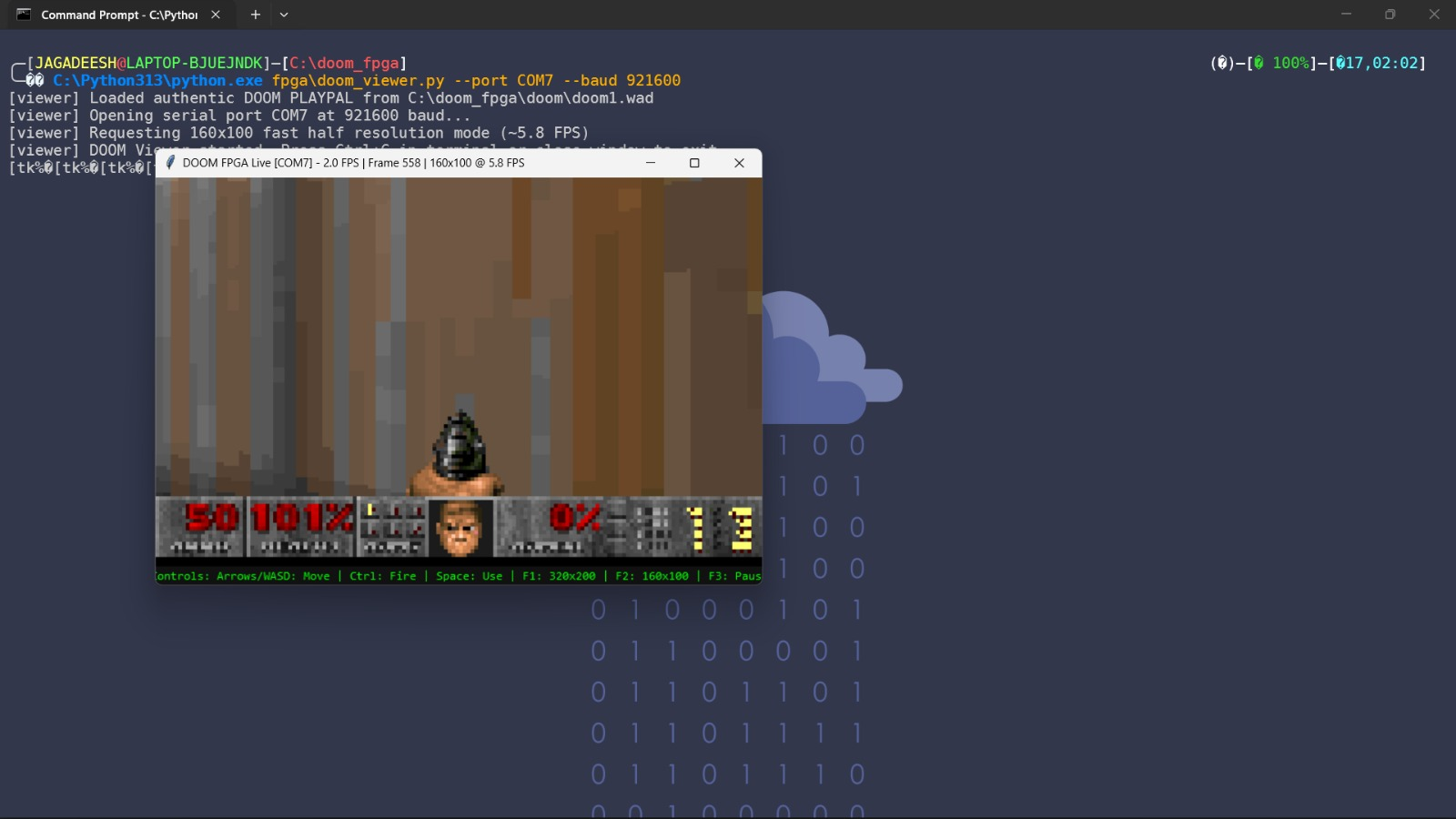
Each frame maps its indices through that palette and upscales nearest neighbor into the 640x400 window, with a measured frames per second figure in the title bar and the controls printed underneath.
| Action | Laptop Key | DOOM Keycode |
|---|---|---|
| Walk Forward | Up Arrow / W | 0xAD |
| Walk Backward | Down Arrow / S | 0xAF |
| Turn Left | Left Arrow / A | 0xAC |
| Turn Right | Right Arrow / D | 0xAE |
| Fire Weapon | Left Ctrl / Right Ctrl | 0xA3 |
| Open Doors / Use | Space | 0xA2 |
| Run / Speed | Shift | 0xB6 |
| Strafe Modifier | Alt | 0xB8 |
| Weapon Selection | Keys 1 through 7 | 0x31 to 0x37 |
| Enter / Menu Select | Enter | 13 |
| Game Menu / Escape | Escape | 27 |
| Automap Toggle | Tab | 9 |
| Full Resolution (320x200) | F1 | 0xFC command |
| Fast Mode (160x100) | F2 | 0xFD command |
| Pause / Resume Stream | F3 | 0xFE command |
Why the display tops out at six frames per second
Five frames per second is not fast enough to feel smooth, and this section will not pretend otherwise. The interesting question is where, exactly, the time goes, because the profiler and the wire disagree, and only one of them limits the game.
Profiling puts a typical frame’s render work near 1.4 million cycles:
$$T_{render} = \frac{1,400,000\ cycles}{50,000,000\ cycles/second} = 0.028\ seconds = 28\ ms$$$$Internal\ Render\ Rate = \frac{1}{0.028\ s} \approx 35.7\ FPS$$The core computes the scene in 28 milliseconds. Then it stays frozen while the wire moves the pixels. At 921,600 baud with 8N1 framing, every byte costs 10 bits on the wire:
$$Bandwidth = \frac{921,600\ bits/second}{10\ bits/byte} = 92,160\ bytes/second\;(\approx 90\ KB/s)$$Full 320x200 carries 64,000 bytes per frame:
$$Transmission\ Time = \frac{64,000\ bytes}{92,160\ bytes/second} \approx 0.694\ seconds$$$$Max\ Throughput = \frac{1}{0.694\ s} \approx \mathbf{1.44\ FPS}$$Fast 160x100 carries 16,000 bytes per frame:
$$Transmission\ Time = \frac{16,000\ bytes}{92,160\ bytes/second} \approx 0.174\ seconds$$$$Max\ Throughput = \frac{1}{0.174\ s} \approx \mathbf{5.75\ FPS}$$So the breakdown is 28 milliseconds of compute followed by 174 milliseconds of wire, per frame, in fast mode. The observed rates land on those lines, which confirms the model matches reality. A parallel VGA DAC at a 25.175 MHz pixel clock would do 60 frames per second; a single async pin is limited to what a single async pin can do, and the frame rate is set by the wire, not the core.
Live visual verification
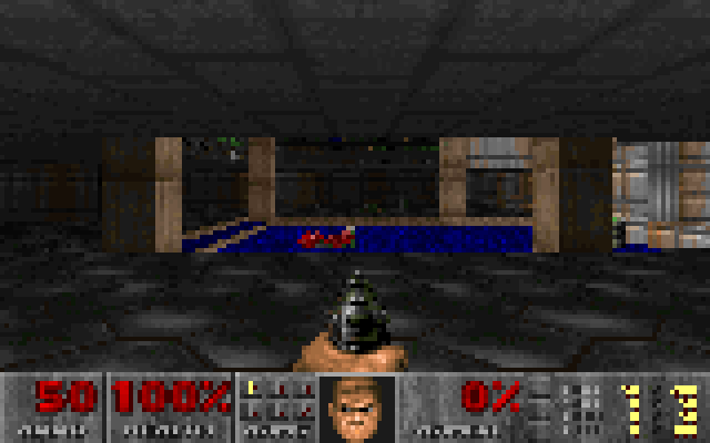
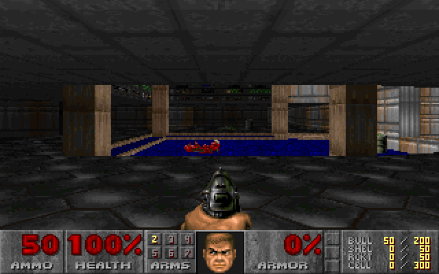
Frames captured directly from the DE0-Nano running live on the desk.
Fast mode (160x100 at about 5.8 FPS), sub-sampled in both dimensions for responsive continuous play:
High resolution mode (320x200 at about 1.4 FPS), full native Mode 13h with status bar numbers and texture detail:
Terminal Screenshot
Making the board a standalone game
The current setup uses the laptop for several parts of the system. The USB-Blaster loads the FPGA design, the CP2102 uploads the ELF and WAD, and the same serial link carries console output, keyboard input, and framebuffer data. A standalone version would move those functions onto the board so that, after programming, it could run from its own power and connect directly to a display and controls.
Booting without the laptop
Programming the FPGA over JTAG is only part of that change. The current bitstream is loaded into volatile configuration memory, and the game image is copied into SDRAM by the serial bootloader. SDRAM contents are lost when the board is powered down, so a standalone version needs both the FPGA configuration and the game image to come from local non-volatile storage.
The DE0-Nano has a 64 Mb configuration flash. The bitstream can be
stored there so the FPGA configures itself at power-up. In Quartus,
that means converting the .sof into the appropriate serial-flash
image and programming the configuration device, rather than loading
only the .sof into volatile FPGA configuration memory. The 4.65 MB
shareware game image could also fit in the remaining space in principle,
but the actual bitstream size and flash layout would need to be checked.
The bootloader would then need a flash read path to copy the ELF and WAD
into SDRAM before releasing the CPU. The configuration flash is not
automatically available as a normal CPU memory window just because it
contains the bitstream, so that read interface is part of the standalone
work.
A separate SPI flash or an SD-card interface would be another option. That would keep the FPGA bitstream in the configuration flash and place the game files in storage intended for application data. For this board, the simplest self-contained arrangement is likely configuration flash for the bitstream and game image, provided the capacity and flash interface are checked first.
Replacing the serial display with VGA
The serial framebuffer path is useful for bring-up, but a physical game would be easier to use with a local display controller. A VGA adapter could be connected to GPIO-0 or GPIO-1 through a small resistor DAC or a VGA add-on board. The controller would generate RGB, HSYNC, and VSYNC, with a PLL providing a pixel clock close to 25.175 MHz for 640x480 at 60 Hz.
The existing framebuffer is 320x200 bytes of palette indices. A simple output mode would scale each pixel by two in both directions, producing a 640x400 image with black borders in a 640x480 frame. The 160x100 mode could use four-pixel scaling if a lower memory bandwidth mode is useful. The VGA path would read each palette index, look up its RGB value from PLAYPAL, and send the resulting colour to the DAC. A 3:3:2 digital RGB output or a small external resistor ladder would be enough for a basic version.
The display reader and the CPU would access the framebuffer at the same time, so the memory path would need an additional arbitration point. A line buffer in M9K memory would let the display controller read a line in advance while the CPU continues rendering into SDRAM. A double buffer would give cleaner frame changes: the CPU renders into one buffer, then the display controller switches to it at vertical blank. For an initial version, a single framebuffer with a swap at the end of a frame would be simpler, although it could show tearing during updates.
With a local VGA reader, the CPU would not need to stop while a frame is transmitted over UART. The game clock could continue normally, and the serial stream could be kept for debugging rather than used as the main display path.
Buttons and controller input
The four onboard pushbuttons are enough for a small test interface, but they do not provide a comfortable DOOM control layout by themselves. A more useful controller would provide at least forward, backward, left, right, fire, use, and run inputs. A small GPIO button board, a PS/2 keyboard interface, or a simple external microcontroller would all be reasonable options. A USB gamepad is possible too, but it needs a USB host interface and a suitable protocol implementation, which is more work than a GPIO or PS/2 input path.
Each button input needs a synchronizer, debounce logic, and held-state tracking. At 50 MHz, a debounce interval in the low-millisecond range is enough for ordinary pushbuttons. The input block should generate a press event and a release event, then hold the current state so that a button can remain active across several game tics. A small event FIFO is useful because two buttons can change close together and the CPU should not lose one while it is polling the key register.
The current guest interface already has the key values needed for a mapper:
- Forward:
0xAD - Backward:
0xAF - Turn left:
0xAC - Turn right:
0xAE - Fire:
0xA3 - Use:
0xA2 - Run:
0xB6 - Strafe modifier:
0xB8 - Weapon keys:
0x31through0x37
The mapper should produce these DOOM key values rather than forwarding
PC scan codes or terminal key codes. With direct GPIO buttons, the FPGA
can translate a button number to a DOOM key value and place the result
in the same key FIFO that DG_GetKey reads. The FIFO entry can contain
the key byte and a pressed or released bit.
The 0xF0 release prefix used by the current serial viewer is only a
transport convention. A direct hardware controller does not need to
send that byte. It can set the release bit directly. If a small
microcontroller is used as the controller, it can send packets such as
key value plus pressed state over a 3.3 volt UART or SPI connection, and
the FPGA can convert those packets into the internal FIFO format.
Powering it from a battery
Once the bitstream and game image are stored locally, the board can be started without the laptop. The practical supply is a regulated 5 V battery pack, a USB power bank, or a single-cell battery followed by a 5 V boost converter connected to the board’s intended power input. A raw battery connection should not be made to the FPGA’s 3.3 V rail or to an arbitrary GPIO pin. The supply should have enough current capacity for the FPGA, SDRAM, display interface, and controller, with some margin for startup and activity.
A power switch can sit between the battery pack and the board input. If the VGA adapter or controller is powered from the same pack, use the appropriate regulated voltage for each device and connect their grounds together. The board’s actual current draw should be measured at the intended clock and workload before estimating battery life. Once the board has configured from flash and copied the game image into SDRAM, the USB-Blaster and CP2102 can be disconnected.
What happens to the CP2102
The CP2102 is not required for the standalone display or input path. It can be unplugged after the FPGA has been configured and the game image has been loaded from local storage. The cleanest arrangement is to remove its TX, RX, and ground connections from the board and keep the module separate for development.
It can also remain as an optional debug port. In that case, the FPGA TX line connects to CP2102 RX, FPGA RX connects to CP2102 TX, and the two systems share a signal ground. The CP2102 power pins should remain unconnected to the FPGA power rail. If the board is running from a battery while the CP2102 is attached to a computer, the two power paths must be kept separate so the USB connection does not back-power the board or conflict with the battery supply.
For an external controller, the CP2102 is usually the wrong permanent interface because it still depends on a host computer. A GPIO, PS/2, SPI, or UART connection to a small controller powered from the same regulated supply is a better standalone input path. The input device and the FPGA should share a ground, and the signal levels should match the FPGA bank voltage.
Choosing between RV32IM and a CPU-free design
For this project, RV32IM is not excessive if the goal is to run the existing doomgeneric code. The CPU handles the game loop, WAD access, BSP traversal, collision checks, thinker updates, weapon state, and renderer. It also makes it possible to change the game in C, load other levels, and reuse the same platform code. The M extension is useful for the fixed-point and geometry calculations, although the current FPGA build uses an iterative unit for most M operations to reduce area.
A CPU-free version is possible, but it would be a different project. It would replace the software engine with hardware blocks for the game tick, player state, input handling, collision, map access, texture and sprite storage, rendering, and framebuffer output. For a fixed E1M1 demo, the map and assets could be stored in ROM or flash, and a specialised raycaster or column renderer could draw directly into the framebuffer. That design could be smaller and more deterministic for one fixed game scenario, but changes to game logic, levels, weapons, or enemies would require changes to the hardware implementation.
The important distinction is that removing the CPU does not leave the same DOOM engine intact. It changes the system from a general-purpose processor running DOOM software into a hardware implementation of a particular game. A CPU is the more practical choice for running the existing source. A CPU-free design makes more sense for a fixed hardware demo where the game behaviour and content are intentionally limited.
A smaller middle ground would keep the RV32IM core, add the VGA controller and local input mapper, and move only the game image into flash. That would remove the serial display bottleneck without requiring a complete hardware rewrite of the game engine.
Summary: the optimisations that made it fit
Neither the core nor the game on the board is the full original. The simulation core needed 29,143 nodes against 22,320 cells, and the Freedoom image needed about 42.6 MB against 32 MB of SDRAM, so both were downscaled to fit: a smaller core running a smaller game, with every downscale verified to change nothing the game computes.
- Predictor tables cut from 256 entries to 16 (
PRED_SMALL): full design registers fell from 23,644 to 6,984 and logic to 17,423 elements (78 percent of the device). - Wide arithmetic replaced by an iterative M unit: MUL-low stays single cycle on the DSP blocks while the other seven M ops run 33 cycles each, at a measured cost of about two percent in game cycles.
- CSR file made synchronous and branch resolution moved from ID to EX: worst slack improved from -14.5 ns to -3.998 ns on the slow corner, and the load-use stall dropped out of the hazard unit.
- One combined
VERILOG_MACROline split in two soPRED_SMALLtakes effect: compile time fell from 17 minutes to 70 seconds. - Freedoom (27.46 MB WAD, 28.11 MB total image) replaced by the
shareware
doom1.wad(4,196,020 bytes, 4.65 MB total): the upload fits the 32 MB SDRAM with about 27 MB of heap headroom. - Serial link retuned from an unsupported 2 Mbaud to 921,600 with ack chunking aligned to payload bytes: the full image uploads in 53 seconds with CRC32 verification.
- Display done over the same wire with the game clock frozen during transfer: 10 byte frame headers, 160x100 fast and 320x200 full modes, and a break protocol for key releases.
Frame 0 stays pixel identical to the reference, the instruction suite matches 46 for 46, and the M1 to M18 micros all pass, so the downscaled system computes the same game.
Conclusion
In simulation, wide arithmetic, predictor tables, memory latency, and the serial link all cost nothing. On the board, each had to be solved as hardware: a 33 cycle M unit, 16 entry predictor tables, a retimed pipeline, a 921,600 baud link with aligned framing, a smaller WAD, and a display path that freezes the game clock during transfer. The whole core fits an entry level Cyclone IV and plays real game code with nothing but a USB serial cable for display, console, and input. Timing remains open on the slow corner; nominal silicon carries it on the bench.
Files
- fpga/rtl/bringup_top.v, uart_tx.v, uart_rx.v, sdram_ctrl.v, sdram_tester.v: phase 1 top, the 8N1 serial pair, the SDRAM controller and its self test.
- fpga/rtl/doom_top.v, mem_top_fpga.v, fifo_sync.v: phase 2 top, the SDRAM backed memory with gated clock, I-cache, bootloader, MMIO, framebuffer streamer, and key decoder, plus the 4 KB UART FIFO.
- fpga/quartus/de0_nano_doom.qpf/.qsf/doom.sdc: device, pins, file list and timing for the EP4CE22 build.
- fpga/uploader.py: info, upload and term at 921,600 baud with payload aligned chunking, CRC verified boot, and a no-term handoff that frees the port for the viewer.
- fpga/doom_viewer.py: threaded serial demux, PLAYPAL render into a 640x400 window, key capture with break codes and mode commands.
- fpga/tb, run_tb.sh, run_doom.sh, mkimage.py: UART, SDRAM and boot benches, the two frame equivalence check and the preload image builder.
- rtl/core: the muldiv diet unit, synchronous CSR with settle stalls, retimed EX hazards, the squash/release fix, and the reset/flush branch split for Quartus.
- micro_gen.py, check_micro.py, tb/gen_md_vectors.py: the M1 to M18 assembly micros and their checkers.