Inside an Op-Amp: CMOS Implementation, Internal Structure, and Non-Idealities
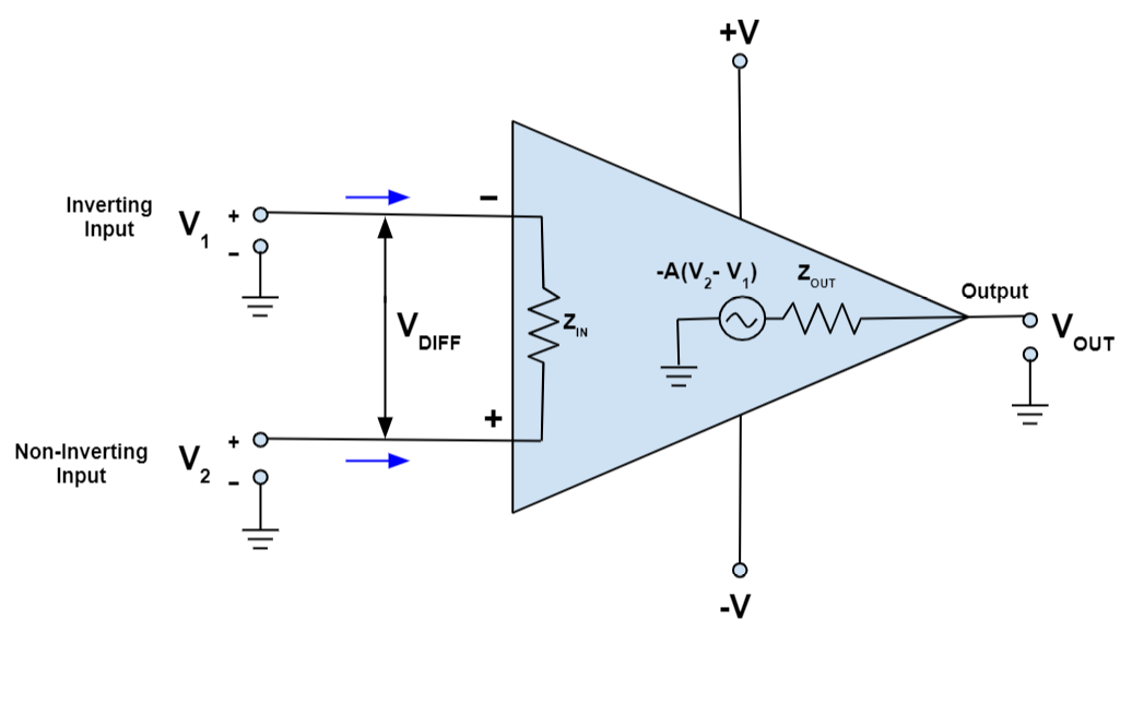
An operational amplifier (op-amp) is a high-gain voltage amplifier with differential inputs and typically a single-ended output. In theory, it provides:
- Infinite gain
- Infinite input impedance
- Zero output impedance
- Infinite bandwidth
In silicon, none of these are true.
Modern op-amps are implemented in CMOS, especially in mixed-signal SoCs and analog front-ends. Understanding their internal structure is critical for:
- ADC driver design
- Active filter implementation
- Feedback stability analysis
- Precision measurement systems
High-Level Block Structure
A typical CMOS op-amp consists of:
- Differential input stage
- Gain stage
- Output stage
- Bias network
- Frequency compensation
Differential Input Stage (CMOS Differential Pair)
The input stage converts differential voltage into current.
Structure
- NMOS or PMOS differential pair
- Tail current source
- Active load (current mirror)
Operation
If \( V_{in+} > V_{in-} \):
- One transistor conducts more
- The other conducts less
- Differential current is generated
Small-signal transconductance:
\[ g_m = \frac{2I_D}{V_{ov}} \]
Where:
- \( I_D \) = drain current
- \( V_{ov} \) = overdrive voltage
Higher \( g_m \) → higher gain.
Why CMOS?
CMOS allows:
- High input impedance
- Low static power
- Integration with digital logic
In modern low-voltage nodes, rail-to-rail input stages often use complementary pairs.
Active Load and Gain Formation
The differential pair feeds into a current mirror load.
Voltage gain of first stage:
\[ A_v = g_m \times r_o \]
Where:
- \( r_o \) is output resistance of MOSFET
High gain requires:
- High output resistance (long channel devices)
- Proper biasing
Short-channel effects reduce \( r_o ), limiting gain in scaled nodes.
Second Gain Stage
The second stage provides additional voltage gain.
Typically:
- Common-source amplifier
- Active load
- High impedance node
Total gain:
\[ A_{total} = A_1 \times A_2 \]
In CMOS:
- 60–100 dB typical open-loop gain
Output Stage
Purpose:
- Drive load
- Provide current amplification
- Reduce output impedance
Common structure:
- Push-pull stage
- Class AB biasing
Output impedance:
\[ Z_{out} \approx \frac{1}{g_m} \]
Lower is better for load driving.
Frequency Compensation
Without compensation, multi-stage op-amps are unstable in feedback.
Solution: Miller Compensation.
A capacitor \( C_c \) is placed between output of first stage and second stage.
This:
- Introduces dominant pole
- Pushes non-dominant poles higher
- Improves phase margin
Unity gain frequency:
\[ f_u = \frac{g_m}{2\pi C_c} \]
Tradeoff:
Larger \( C_c ):
- More stable
- Slower bandwidth
Real-World Non-Idealities
An op-amp is fundamentally nonlinear due to device physics.
Key non-linearities include:
- Input offset voltage
- Finite gain
- Slew rate limitation
- Output swing limitation
- Input bias current
- Common-mode rejection limits
- Power supply rejection limits
Input Offset Voltage
Defined as the input voltage required to make output zero.
Caused by:
- Threshold mismatch
- Current mirror mismatch
- Device mismatch (Pelgrom model)
\[ V_{os} \propto \frac{A_V}{\sqrt{W \times L}} \]
Larger devices reduce mismatch.
Offset affects:
- Precision ADC drivers
- Instrumentation amplifiers
Slew Rate
Slew rate is the maximum rate of change of output voltage:
\[ SR = \frac{I_{bias}}{C_c} \]
When input step is large:
- Differential pair saturates
- Tail current fully steered
- Output capacitor charged/discharged at constant current
Result:
- Linear ramp instead of exponential
Large signal response is current-limited, not gain-limited.
High slew rate requires:
- Larger bias current
- Smaller compensation capacitor
Tradeoff:
- Higher power consumption
Finite Open-Loop Gain
Ideal assumption:
\[ A \to \infty \]
Real:
\[ A = 10^4 \text{ to } 10^6 \]
In closed loop:
\[ A_{cl} = \frac{A}{1 + A\beta} \]
Finite gain introduces gain error.
Important in:
- Precision filters
- Data converter drivers
Gain Bandwidth Product (GBW)
For single dominant pole:
\[ GBW = A_0 \times f_p \]
Closed-loop bandwidth reduces as gain increases.
High-speed systems require high GBW.
Output Swing Limitation
CMOS output stage cannot reach rails fully.
Due to:
- \( V_{DSsat} )
- Headroom constraints
Rail-to-rail output requires special architectures.
Common-Mode Range
Input common-mode range is limited by:
- Tail current source headroom
- Threshold voltages
- Saturation region requirements
In low-voltage designs, this becomes critical.
Distortion
Nonlinearity in:
- Transconductance
- Output stage
- Capacitive loading
Harmonic distortion increases with:
- Large signal amplitude
- Insufficient bias current
Total Harmonic Distortion (THD):
\[ THD = \frac{\sqrt{V_2^2 + V_3^2 + …}}{V_1} \]
Critical for:
- Audio
- High-resolution ADC drivers
Noise
Major sources:
- Thermal noise
- Flicker noise (1/f)
- Current mirror noise
Input-referred noise:
\[ e_n^2 = \frac{4kT\gamma}{g_m} \]
Higher \( g_m \) reduces noise.
Tradeoff:
- Higher current → more power
Power Supply Rejection Ratio (PSRR)
PSRR indicates how well op-amp rejects supply variations.
Low PSRR:
- Supply ripple leaks into output
- ADC reference accuracy degrades
Improved by:
- Cascode structures
- Bias isolation
Stability and Phase Margin
Phase margin must typically exceed:
\[ 45^\circ \text{ to } 60^\circ \]
Low phase margin:
- Ringing
- Oscillation
- Poor transient response
Compensation design is critical.
Final Engineering Perspective
An op-amp is not a black box.
It is a carefully balanced system of:
- Transconductance devices
- Current mirrors
- High impedance nodes
- Compensation networks
- Bias circuits
Improving one metric often degrades another:
- Higher gain → lower bandwidth
- Higher slew rate → higher power
- Lower noise → larger devices
Analog design is constraint optimization.
In mixed-signal systems, especially ADC front-ends, the op-amp often defines system-level performance more than the digital backend.
Understanding internal CMOS structure enables:
- Better stability design
- Accurate distortion budgeting
- Correct noise modeling
- Robust analog front-end integration