Inside an Op-Amp: CMOS Implementation, Internal Structure, and Non-Idealities
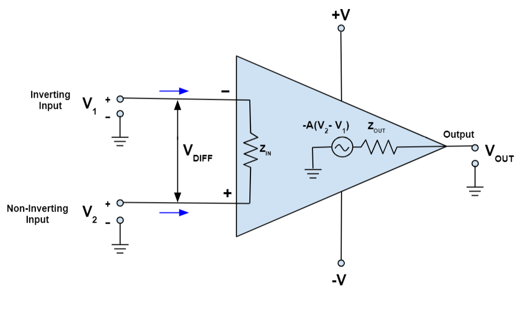
A CMOS operational amplifier is a multi-stage analog circuit that achieves high voltage gain, high input impedance, and controlled frequency response through a specific arrangement of differential pairs, current mirrors, and compensation networks. The textbook model of an op-amp, with infinite gain and zero output impedance, is a useful fiction for circuit analysis. Designing with real CMOS op-amps, or designing the op-amp itself, requires understanding the transistor-level structure that produces the specifications on the datasheet and the mechanisms by which those specifications degrade under real operating conditions.
This post covers the internal structure of a standard two-stage CMOS op-amp, the function of each stage, the compensation technique that makes multi-stage designs stable in feedback, and the non-ideal effects that limit performance.
Differential Input Stage
The first stage of a CMOS op-amp is a differential pair, typically a matched pair of PMOS or NMOS transistors with a shared tail current source. The differential pair converts a small differential voltage at its inputs into a differential current at its outputs, while rejecting common-mode voltage changes that affect both inputs equally.
In the PMOS differential pair configuration, the two matched transistors M1 and M2 have their sources connected to a tail current source $I_{SS}$ and their drains connected to an active load. When the two gate voltages are equal, the tail current splits equally between M1 and M2. When a differential voltage $V_{id} = V_{in+} - V_{in-}$ is applied, the current splits asymmetrically, with one transistor conducting more and the other less, in proportion to the transconductance.
The small-signal transconductance of the differential pair is:
$$ g_m = \sqrt{2\mu_p C_{ox} (W/L) I_D} $$where $\mu_p C_{ox}$ is the process transconductance parameter for PMOS, $W/L$ is the transistor aspect ratio, and $I_D = I_{SS}/2$ is the quiescent drain current of each transistor. Transconductance increases with bias current and with transistor size, but both come at cost: higher bias current increases power, and larger transistors increase parasitic capacitance, which limits bandwidth.
The active load is a current mirror formed by transistors M3 and M4. The current mirror copies the current from one drain to the other, converting the differential current into a single-ended current at the output node. The conversion is necessary because the second gain stage is a single-ended common-source amplifier. Without the current mirror load, the differential pair’s output would need to be recombined, which complicates the circuit and reduces the gain. With the current mirror, the output current is $g_m V_{id}$ flowing into a high-impedance node, and the first-stage voltage gain is:
$$ A_{v1} = g_m (r_{o2} \| r_{o4}) $$where $r_{o2}$ and $r_{o4}$ are the output resistances of M2 and M4, the two transistors that are both conducting their drain currents into the same output node. The output resistance of a MOSFET in saturation is $r_o = 1/(\lambda I_D)$, where $\lambda$ is the channel-length modulation parameter. $r_o$ increases with channel length and decreases with bias current. Long-channel devices provide high output resistance and therefore high gain, at the cost of larger area and reduced bandwidth due to larger parasitic capacitances.
In short-channel processes, the channel-length modulation effect is stronger: $\lambda$ is larger, $r_o$ is smaller, and the gain achievable from a single differential pair stage is substantially reduced compared to a long-channel process. This is one reason why two-stage op-amp designs are more common than single-stage designs in modern processes, and why cascode structures are used to boost effective output resistance when high gain is required.
Common-Mode Rejection and Input Range
The differential pair rejects common-mode input changes because a voltage that moves both inputs equally does not change the differential current $g_m V_{id}$, it only slightly modulates the tail current through the finite output resistance of the tail current source. The common-mode rejection ratio (CMRR) is determined by how well the tail current source suppresses common-mode variations:
$$ CMRR \approx g_m \cdot r_{o,tail} \cdot A_v $$A high-impedance tail current source, typically implemented as a cascode current mirror, provides high $r_{o,tail}$ and therefore high CMRR. A simple single-transistor tail current source has lower output resistance and degrades CMRR.
The input common-mode range is the range of voltage at the input terminals over which the differential pair operates correctly. For a PMOS pair with a tail current source pulling the sources toward the supply, the input common-mode range extends from somewhat below the positive supply rail down to a minimum voltage set by the requirement that the tail current source and the differential pair transistors remain in saturation. If the common-mode input drops too low, the tail current source leaves saturation and the bias current becomes incorrect. In low-voltage processes where the supply is 1.8V or lower, maintaining adequate common-mode range requires careful biasing and may require a complementary input stage using both NMOS and PMOS pairs to cover the full rail-to-rail range.
Second Gain Stage
The second stage is a common-source amplifier with an active load. The output of the first stage drives the gate of a NMOS transistor M5, whose drain is connected to a PMOS current source load M6. The voltage gain of this stage is:
$$ A_{v2} = g_{m5} (r_{o5} \| r_{o6}) $$The total open-loop gain of the two-stage op-amp is $A_v = A_{v1} \cdot A_{v2}$. With both stages contributing 30 to 50 dB of gain, total open-loop gain of 60 to 100 dB is achievable in standard CMOS processes.
The second stage also has high output resistance, which is useful for driving other high-impedance loads but is a problem when the output must drive a resistive load or a large capacitance. Driving a resistive load from a high-impedance second stage creates a load-dependent gain: as the load resistance decreases, the effective output resistance decreases and the gain drops. A dedicated output stage is added when the op-amp must drive low-impedance loads.
Miller Compensation
A two-stage op-amp without compensation has two significant poles: one at the output of the first stage (determined by the capacitance to ground at that node and the first stage output resistance), and one at the output of the second stage. When used in a feedback configuration, a system with two poles can become unstable or exhibit excessive ringing depending on the relative frequencies of the poles and the unity-gain frequency of the loop.
Miller compensation adds a capacitor $C_c$ connected between the input and output of the second stage. This capacitor has two effects. First, it introduces a zero in the right half plane at:
$$ f_z = \frac{g_{m5}}{2\pi C_c} $$which degrades phase margin. Second, through the Miller effect, it appears as a much larger capacitance at the output of the first stage, because the gain of the second stage multiplies the capacitance. The effective capacitance at the first stage output is approximately $C_c(1 + A_{v2})$. This large effective capacitance pushes the first-stage pole to a much lower frequency:
$$ f_{p1} = \frac{1}{2\pi R_{out1} C_c A_{v2}} $$At the same time, the second-stage pole is pushed to a higher frequency because the compensation capacitor adds a low-impedance path from the second stage output, reducing the effective impedance seen at that node. The result is pole splitting: the dominant pole moves to low frequency, the non-dominant pole moves to high frequency, and the unity-gain frequency of the op-amp falls between them.
The unity-gain frequency is:
$$ f_u = \frac{g_{m1}}{2\pi C_c} $$For the op-amp to be stable in unity-gain feedback, the non-dominant pole must be at a frequency higher than $f_u$. The required phase margin, typically 45 to 60 degrees, determines how much higher the non-dominant pole must be relative to $f_u$, and therefore constrains the minimum value of $C_c$. A larger $C_c$ provides better phase margin but reduces $f_u$ and therefore reduces the closed-loop bandwidth of any feedback circuit using the op-amp.
The right-half-plane zero introduced by $C_c$ degrades phase margin and must be addressed. One approach is to add a resistor $R_z$ in series with $C_c$, which shifts the zero location. Choosing $R_z = 1/g_{m5}$ places the zero at infinity, eliminating it entirely. A value of $R_z$ slightly larger than $1/g_{m5}$ moves the zero to the left half plane, where it adds phase lead and can actually improve phase margin if placed correctly.
Input Offset Voltage
In a perfect differential pair, equal input voltages produce equal drain currents and the output is at the correct quiescent value. In a real circuit, transistor threshold voltages vary randomly from device to device due to process variation. The matched transistors M1 and M2 have slightly different threshold voltages, and similarly M3 and M4 in the current mirror load have slightly different characteristics. These mismatches mean that equal input voltages produce an output that is offset from the ideal value, as if there were a small differential input voltage applied. This is the input offset voltage $V_{os}$.
The offset magnitude follows the Pelgrom model for transistor mismatch:
$$ \sigma(V_{os}) \propto \frac{A_{VT}}{\sqrt{WL}} $$where $A_{VT}$ is the technology-dependent threshold voltage mismatch coefficient (typically a few mV·μm) and $WL$ is the gate area of the matched transistors. Larger transistors have smaller mismatch. Doubling the gate area reduces the standard deviation of offset by $\sqrt{2}$. This is why precision analog circuits use large transistors in the input stage despite the area cost: the achievable offset directly limits the precision of the amplifier in DC applications.
In a 12-bit ADC driver, the allowed offset after gain correction is on the order of $V_{ref}/2^{12} \approx 1.2$ mV for a 5V reference. Achieving this without trimming requires input transistors large enough that the process mismatch produces offset below this level with high probability across the production distribution, which typically means transistors with gate areas of several hundred square microns, substantially larger than minimum-sized transistors.
Slew Rate
The slew rate is the maximum rate of change of the output voltage, limited by the maximum current available to charge or discharge the load capacitance. For the two-stage op-amp with Miller compensation capacitor $C_c$:
$$ SR = \frac{I_{SS}}{C_c} $$Under small-signal conditions, the output voltage follows the input smoothly according to the bandwidth of the closed-loop system. Under large-signal conditions, when the input step is large enough to fully steer the tail current to one side of the differential pair, the available current into $C_c$ is limited to $I_{SS}$, and the output charges at a constant rate rather than exponentially. This current-limited behavior is the slew rate, and the output waveform during slewing is a linear ramp rather than an exponential approach.
The consequence for circuit design is that the slew rate and the gain-bandwidth product are linked by the compensation capacitor, but in opposite ways. Increasing $C_c$ improves stability (better phase margin) but reduces both the unity-gain bandwidth and the slew rate. Increasing $I_{SS}$ improves slew rate (and also increases $g_m$, which increases $f_u$) but increases power. For a given power budget, the designer must balance slew rate against stability margin.
In an ADC driver application where large signal steps are common, insufficient slew rate causes the output to take longer to reach its final value than the allowed settling time, directly reducing the effective resolution of the ADC. The driver must be sized with a slew rate that allows the output to reach within $\Delta/2$ of the final value within the acquisition window, and the bias current must support this slew rate while also satisfying the noise requirement.
Noise
The dominant noise sources in a CMOS op-amp are thermal noise and flicker (1/f) noise.
Thermal noise in a MOSFET channel is modeled as a current noise source at the drain with spectral density:
$$ \overline{i_n^2} = 4kT\gamma g_m $$where $\gamma$ is a process-dependent constant (approximately 2/3 for long-channel devices, higher for short-channel) and $g_m$ is the transconductance. Referred to the input, this becomes a voltage noise with spectral density $4kT\gamma / g_m$. Higher transconductance reduces input-referred noise, which is why high-performance op-amps use high bias currents in the input stage.
Flicker noise (1/f noise) originates from carrier trapping and detrapping at the oxide-semiconductor interface. Its power spectral density is inversely proportional to frequency, so it dominates at low frequencies. The corner frequency where flicker noise equals thermal noise is typically in the kHz to MHz range for CMOS processes. For audio and precision DC applications, flicker noise in the input stage is the primary noise concern. PMOS transistors typically exhibit lower flicker noise than NMOS in most CMOS processes, which is one reason PMOS input stages are common in precision op-amps even when NMOS would provide higher $g_m$ for the same bias current.
The noise of the active load transistors M3 and M4 also contributes to the input-referred noise. This contribution is approximately equal to the contribution from M1 and M2 when the transconductances are matched, which roughly doubles the noise compared to a simple resistive load. Cascoding the active load, which is done in some high-performance designs, does not reduce this noise contribution because the cascode transistors are in the signal path.
Power Supply Rejection
Power supply rejection ratio (PSRR) describes how effectively the op-amp’s differential gain rejects variations in the supply voltage. A variation $\Delta V_{DD}$ on the supply that appears at the output as $\Delta V_{out}$ gives a PSRR of $\Delta V_{out} / \Delta V_{DD$ referred to the input.
Supply variations reach the output through several paths: through the tail current source (if its output resistance is finite, a supply variation modulates the tail current and therefore the output), through the PMOS current source in the second stage (which sets the quiescent current and output voltage), and through direct capacitive coupling from supply to high-impedance nodes. The Miller compensation capacitor provides a path for high-frequency supply noise to reach the compensation node, which degrades PSRR at high frequencies.
A well-designed op-amp achieves 60 to 80 dB of PSRR at DC through high-impedance current sources and cascode structures. PSRR degrades with frequency, typically at 20 dB per decade above the dominant pole, because the feedback loop that suppresses supply variations requires gain that decreases at high frequencies. In a high-precision ADC reference driver application, PSRR at the switching frequencies of nearby digital circuits is often the binding constraint, and layout techniques such as separate supply routing, shielding, and substrate contact placement are used alongside the circuit design to meet the system’s noise budget.