Reverse Engineering the Jane Street ASIC Puzzle


Jane Street released an ASIC reverse engineering puzzle in August 2026. They taped out a chip on the SkyWater 130 nm open PDK and published the final GDS, plus an example VCD showing some inputs and outputs. The goal is to find the serial input sequence that makes the success output go high, then read off the ASCII string the chip prints
This post walks through extracting a Verilog netlist from the GDS, verifying it against the VCD, and using a formal model checker to recover the 121-bit input that asserts success. The SMT solver run that produced the answer took under two minutes on a laptop. Getting to a netlist the solver would actually consume took a few evenings of iterating between KLayout and the extractor script, checking a mismatch in one, adjusting the other, rerunning
TL;DR
The chip is a two-star Star Battle verifier on an 11x11 grid. It reads 121 bits of serial input, then checks five things:
- Exactly 22 stars (ones) in total.
- Exactly two stars per row.
- Exactly two stars per column.
- No two stars adjacent in any of the eight directions.
- Exactly two stars per hidden region, where the 11 regions spell out “JS” across the die.
When all five conditions hold, success asserts on cycle 126 and the output ROM prints (* TWO STARS *). The answer string is TWO STARS
.......*.*.
*....*.....
.......*.*.
*.*........
....*.*....
..*.....*..
....*.....*
.*....*....
...*......*
.....*..*..
.*.*.......
The design responds to a few input classes with different messages. All-zeros prints EMPTY SKY. All-ones prints BIG BANG. Two per row and column but adjacent stars prints TWO NOT TOUCH. Anything else prints TRY AGAIN, which matches the example VCD
| Input | Output |
|---|---|
| All zeros | EMPTY SKY |
| All ones | BIG BANG |
| 2/row+col but touching | TWO NOT TOUCH |
| Other wrong input | TRY AGAIN |
| Correct solution | (* TWO STARS *) |
The design uses 738 standard cells from the SKY130 sky130_fd_sc_hd library. Cell instance names are preserved in the GDS, which keeps this in the realm of netlist recovery rather than true transistor-level reverse engineering
First look
The repo ships four items: puzzle.gds, example_inputs.vcd, layout.png labeling the major regions, and a warmup/ folder containing the Verilog source, synthesized netlist, placed-and-routed DEF, and final GDS for a small adder/comparator. I spent the first evening doing nothing more complicated than opening the GDS in KLayout and reading through the VCD with less
The VCD header makes the top-level interface obvious:
$var reg 1 ! clk    $end
$var reg 1 " rst_n  $end
$var reg 1 # enable $end
$var reg 1 $ I      $end
$var wire 8 % O [7:0] $end
$var wire 1 & success $end
Clock, active-low reset, enable, one bit of serial input I, an 8-bit output bus O, and a success wire. After reset and a serial feed, O changes one byte per clock:
#1255000  b1010100 %     T
#1265000  b1010010 %     R
#1275000  b1011001 %     Y
#1285000  b100000  %     space
...
The bytes spell TRY AGAIN, followed by a null terminator, an idle gap, then the message repeats. The timing pattern is three cycles of reset, one cycle idle, then 121 cycles with enable high and I shifting in bits, then enable drops and the bytes stream out
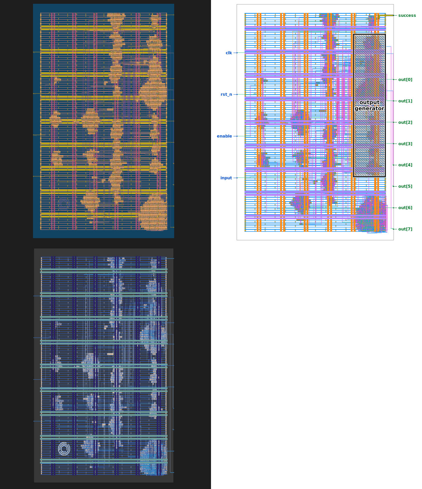
In KLayout the die is visible as a sea of standard cells with a prominent horizontal VDD/VSS strap grid on the upper metals. Cycling through metal layers in KLayout makes it clear that met5 is almost entirely a power grid, met4 has a few long vertical routes plus power, and signals mostly live on met1 through met3 with vias hopping up to met4 for longer runs. The cell placement itself is spatially structured: there are clear rectangular blocks, one dense column on the right, two flop banks in the middle, and a small dense block in the top-right corner that turns out to be the output ROM
I opened the warmup GDS at the same time and ran the same visual inspection. The warmup is 27 cells and the source Verilog is provided, so it gives you a ground truth to check any extraction work against
Cell inventory
The warmup Verilog instantiates sky130_fd_sc_hd__* cells. That told me which PDK to pull and that cell names in the GDS correspond directly to standard-cell functions (nand2_2 is a 2-input NAND size-2, dfxtp_2 is a positive-edge D flop, and so on)
The first gdstk script walked the top-level cell references and counted instances by name
import gdstk
lib = gdstk.read_gds("puzzle.gds")
top = lib.top_level()[0]
counts = {}
for ref in top.references:
    name = ref.cell_name
    if name.startswith("sky130_fd_sc_hd__"):
        counts[name] = counts.get(name, 0) + 1
The first pass returned 412 cells, which looked low. Looking at the reference objects, a lot of them are AREFs (array references) that the pad ring and fill-cell rows use; gdstk does not automatically expand array references into individual instances. Walking ref.ref_cell.references recursively and applying the array replication brought the count up to the 738 that matches other public writeups
The SKY130 library contains a lot of physical-only cells that appear in the placed GDS but carry no logic function: tap cells for well ties, fill cells for density, decaps, antenna diodes, endcaps. The warmup DEF and LEF both show these cells present in placement but absent from the netlist, so the approach is to filter them by name prefix. Building that filter list was iterative. Taps, fills, decaps, and endcaps are obvious. Clock buffer cells (clkbuf_*) are also on the physical side for functional extraction purposes: they are sized inverters on the clock distribution tree, and while they do drive clock pins, they do not change the logical function. Leaving them in the instance list is harmless if you have accurate behavioral models for them, but the first set of primitives I pulled from the PDK did not include models for the antenna-diode variants, which produced floating outputs downstream. Treating clkbuf as a pass-through (drop the instance, connect its input net directly to its output net names) keeps the clock tree intact without requiring those models
One category that does not belong on the physical-only list is conb, the constant-0/constant-1 driver cell. These cells source tie signals to reset pins and unused gate inputs. The first filter put conb in the physical-only bucket along with taps and fills, which produced a netlist where several flop reset pins had no driver and their state bits resolved to X in simulation. The X propagation itself was what pointed back at the tie cells: in a design this dense, a handful of undriven inputs showing up as X is normal (pull-ups/downs, analog pins), but whole columns of flops going X on reset suggested a missing driver. Looking at the LEF for the reset-pin driver cells on one of those flops traced back to a conb instance in the GDS at the expected location
Once the filter was correct, the placed cell origins paint a clear picture of the floorplan. Coloring cells by function (flops vs combinational vs clock-related) reproduces the block layout visible in layout.png: two horizontal flop banks in the center (the bit storage for row state and column state), a dense combinational block between them (the adjacency checker), a vertical counter column on the lower right (the 0-121 epoch counter plus the total-22 star counter), and a small block top-right (the output ROM)
Net extraction
The problem from here is determining which pins on which cells are electrically connected. The options I considered were (1) importing the GDS into KLayout and running its built-in net tracer, and (2) building a polygon-based extractor in Python against gdstk and shapely
The KLayout tracer requires a properly configured technology file with layer mapping and LEF macro descriptions, and my attempts to point it at the raw SKY130 tech file from the PDK produced errors I did not want to chase before even looking at the puzzle logic. I went with the polygon-based approach on the guess that it would be easier to debug, full control over what “connected” meant at each step, at the cost of writing more of it myself. That trade-off held up in practice, though I never pushed the KLayout path far enough to say whether it would have worked too
The idea:
- Read every polygon on every metal layer and every via layer
- Merge overlapping and abutting polygons on the same layer into one shape per connected net fragment
- For each via cut, find the metal polygons above and below that intersect the via and union those fragments
- Transitive closure of those unions across layers produces nets
Step 2 took a few iterations to get right. Reading individual GDS rectangles directly and then looking for overlaps works for narrow signal wires but misses power straps, which are built from many adjacent rectangles that touch at edges rather than overlap. Treating edge-adjacent polys on the same layer as connected is what shapely.unary_union does for free; running it once per layer produces one MultiPolygon per metal layer where each member is a fully connected fragment. Without that pre-merge step, the extractor produced tens of thousands of fragments (one per drawn rectangle) instead of hundreds of connected shapes, and the union-find spent minutes merging things that should have been one shape
Layer mapping was its own rabbit hole. GDS layers are identified by integer (layer, datatype) pairs. The LEF refers to layers by name (metal1, via1, etc.). The SKY130 mapping is publicly documented, but the first mapping I used came from an old project fork and had via3 at the wrong datatype. Signals on the design are short enough that most routing stays on met1-met3, so the error did not produce obvious breakage for short nets; the symptom was about a dozen pins that appeared unconnected on the upper part of the die, mostly long vertical routes that hop up to met4. The single-driver check I ran after pin matching flagged a handful of output pins that appeared to have no route to their load pins, and tracing those routes manually in KLayout showed they crossed met3/met4 at via3 positions where my extractor saw no connection. Pulling the canonical layer map from the PDK’s own layers.lyp file resolved the discrepancy
The GDS uses 1 nanometer database units; the LEF describes pin geometry in microns. Multiplying LEF coordinates by 1000 converts to DBU, but fractional microns in the LEF (0.0005 um is one half-DBU) produce floats like 12959.999999999998 after multiplication, which shapely then treats as distinct from the integer grid. Intersection tests against polygons drawn on integer nanometer boundaries can miss pins by that epsilon, producing pins that appear to float. Casting LEF rectangles to integer nanometers after multiplication (with a single consistent rounding direction) keeps everything on the same grid
Power and ground are huge continuous grids spanning the die. They connect to VPWR and VGND pins on every cell. Rather than trying to identify them by label text (labels in the GDS only appear in a few places and do not cover the whole grid), the approach that worked was to run union-find across all layers, compute the total polygon area of each resulting net, and drop the two largest nets. Those are always VDD and VSS on a design this size, and they dwarf every signal net by two orders of magnitude in area
The text labels for top-level IO ports (clk, rst_n, enable, I, O[0] through O[7], success) are attached to polygons on various layers, not always on the top metal. Iterating over every text element in the top cell regardless of layer and joining it to whatever net polygon it overlaps labels all of them; restricting the search to met4 labels missed the lower half of the output bus
The union-find itself is standard:
parent = {}
def find(x):
    while parent[x] != x:
        parent[x] = parent[parent[x]]
        x = parent[x]
    return x
def union(a, b):
    ra, rb = find(a), find(b)
    if ra != rb:
        parent[rb] = ra
Each merged polygon on each layer gets a unique integer id and starts as its own set. Vias look up the polygon ids above and below in shapely STRtrees (built once per layer for the merge step) and union them. STRtree is what keeps the extractor fast; the naive O(N^2) intersection test was minutes per run, and STRtree drops it to seconds
Cell pin matching
With net fragments identified, the next step is to map each cell pin to a net. The geometry for that lives in the PDK LEF: each macro describes its pins as a set of rectangles on specific layers
The first LEF I pointed the script at was sky130_fd_sc_hd.tlef, the technology LEF that ships with the PDK. That file contains layer definitions, blockages, and routing obstructions but no pin geometry, which my script did not catch because it was reading macros and iterating their pin lists without checking whether any rectangles were present. The result was a pin matcher that ran to completion and reported that about 90% of signal pins did not intersect any polygon. I assumed for a while that this meant my net extraction was missing met1 routing, but when I diffed the warmup extraction (where pin positions are known from the source Verilog) the same 90% miss rate showed up, at which point I looked at the LEF file directly and saw that pin shapes were absent. Switching to the full macro LEF under libs.ref/sky130_fd_sc_hd/lef/ provided the rectangles
For each placed cell, the matcher iterates over signal pins, translates each pin rectangle by the cell origin (applying rotation where the cell is placed rotated), and intersects the translated rectangle against the STRtree of merged polygons on that pin’s layer
Several cells in the SKY130 library, particularly higher drive-strength outputs, have pins split across multiple rectangles. The output pin on a size-4 NAND, for example, is a comb shape with fingers reaching several routing tracks, and each finger is its own RECT entry in the LEF. If you stop at the first intersecting rectangle, pins that only touch metal through a second finger appear unconnected. Iterating over all rectangles per pin and unioning any nets they touch handles that, since electrically all rectangles of the same pin are the same node
Cells in the output ROM block are placed with 90-degree rotation. KLayout shows them clearly as a grid oriented perpendicular to the main standard-cell rows. The first pass of pin matching applied only the origin translation without rotation; those cells’ pins all appeared to float or connect to the wrong nets, and the output bytes from simulation came out garbled (recognizably ASCII, but the wrong characters). Applying the rotation matrix from ref.rotation to the pin coordinates around the cell origin before translation resolved those cells
After each iteration of the matcher, I ran a single-driver sanity check: each output pin (X on combinational gates, Q/Q_N on flops) must drive exactly one net, and each net may have at most one output driver. Multi-driver conflicts and zero-driver inputs flagged specific places to look rather than waiting for simulation to produce X
Emitting Verilog
With the connection table populated, emitting Verilog is mechanical. Nets get sequential names net<N>, the labeled IO nets get their port names, and each cell instance becomes a structural instantiation with its port connections
module puzzle(
    input wire clk,
    input wire rst_n,
    input wire enable,
    input wire I,
    output wire [7:0] O,
    output wire success
);
// ...
sky130_fd_sc_hd__nand2_2 u_201 (
    .A(net134),
    .B(net88),
    .Y(net135)
);
sky130_fd_sc_hd__dfxtp_2 u_418 (
    .CLK(clk),
    .D(net542),
    .Q(net412)
);
// ...
endmodule
For functional simulation the structural netlist needs behavioral models for each cell. The SkyWater PDK ships these as Verilog primitive UDP models (primitives.v, sky130_fd_sc_hd.v, and the UDP definitions). Pulling those in gives a simulatable model without transistor-level simulation
Verifying against the example VCD
Before trying to solve anything, the netlist has to reproduce the provided VCD. I built a Verilator testbench that replays the exact reset and bit sequence from example_inputs.vcd and prints O bytes as they appear
The first runs produced X on several state bits. The cause was the conb filter issue described earlier. After fixing that, the simulation ran without X but the printed bytes did not match: TRY AGAIN came out with a garbled third character in some runs and X in others, which narrowed the problem to one of the O bits. The VCD waveform shows O[3] transitioning at the third character; tracing that bit back through its driver tree to its driver cell, the pin on that cell did not match to any net in the extracted netlist. Looking at the LEF for that specific cell, its output pin rectangle sat at a position whose Y coordinate, after the LEF-to-nanometer conversion, had landed at a half-integer due to a 0.5 nm rounding error, and the intersection test against the integer-coordinate metal polygons was jittering between two adjacent polygons depending on polygon order in the STRtree. The integer snap described earlier (consistent rounding direction when converting LEF microns to DBU) resolved it
The other verification issue was the clock buffer antenna diodes. The LEF distribution I initially used was the “antenna diode removed” variant that ships with some PDK configurations for reduced file size. The clkbuf cells in that LEF have their input pins defined but the diode pins stripped, while the GDS contains the diode cells physically attached. The extractor saw the diode instances and tried to match their pins, found no LEF entry for some of them, and the clkbuf outputs ended up driving nets that also had floating diode pins attached. Rather than track down a matching LEF, the simpler fix was the one mentioned earlier: treat clkbuf as logically transparent and replace each clkbuf instance in the netlist with a direct wire from its input net to its output net
After those fixes, the simulated O bytes matched the VCD exactly through both TRY AGAIN repetitions and the idle gap between them, with success low throughout. A diff of the simulated byte stream against a VCD-parsed reference showed no differences
Solving: cover(success)
At this point I had a trusted netlist. The question was how to get the answer out. I spent an hour probing internal signals in simulation to understand the structure before settling on formal verification
Watching internal counters while feeding the example bitstream, a few things are visible immediately. A counter increments every clock and wraps at 121; that is the bit counter. A secondary counter increments every 11 clocks (mod 11), which means the design is treating the input as 11 groups of 11, i.e. rows of a grid. A set of flops in the upper flop bank saturates when a row has seen two 1s; another set in the lower bank saturates per column. An 8-bit counter on the lower right totals the number of 1s seen and compares against 22
The constant 22 and the 11x11 grid structure pointed at Star Battle (22 stars on 11x11, two per row). The combinational block between the flop banks holds a shift register that checks bits in a small window around the current position, which matches the eight-direction adjacency rule. I identified those structures by adding debug prints to the Verilator testbench and watching which comparators fired on all-zeros vs all-ones vs a hand-constructed “two per row/col but touching” input. Those three inputs produced three different messages (EMPTY SKY, BIG BANG, TWO NOT TOUCH), which mapped cleanly to three of the five checks failing
I considered writing a brute-force enumerator for the 2/row + 2/col + 22-ones + no-adjacent constraint set, but a few minutes of thinking suggested that set alone admits thousands of solutions (a standard 11x11 two-star Star Battle without region constraints has many solutions; the fifth per-region constraint is what makes it unique). That fifth constraint, whatever it was, sat in a block I had not fully decoded (Box 10, the magic_index LUT). Rather than fully reverse-engineer that LUT by hand, formal verification can answer the question directly from the netlist
SymbiYosys can take a Verilog design and ask “is there an input sequence that causes property P to hold,” and it hands the unrolled circuit to an SMT solver to search for a witness. The property here is cover(success)
The harness declares a free 121-bit input vector, feeds it in bit by bit following the reset and enable sequence observed in the VCD, and asks the solver to cover success
module sby_wrapper(input clk);

(* anyconst *) wire [120:0] input_data;

reg [8:0] counter = 0;
reg rst_n;
reg enable;
reg I;
wire success;
wire [7:0] O;

puzzle p(
  .clk(clk),
  .rst_n(rst_n),
  .enable(enable),
  .I(I),
  .O(O),
  .success(success)
);

always @(*) begin
  rst_n  = 1;
  enable = 0;
  I      = 0;
  if (counter < 3) begin
    rst_n = 0;
  end else if (counter < 4) begin
    rst_n = 1;
  end else if (counter < 4 + 121) begin
    enable = 1;
    I = input_data[counter - 4];
  end
  cover(success);
end

always @(posedge clk) begin
  counter <= counter + 1;
end
endmodule
The timing in the harness mirrors the VCD exactly: three cycles in reset, one idle cycle with rst_n high and enable low, then 121 cycles shifting bits, then enable drops. Getting that sequence wrong was a real concern because the state machine that waits for the 121 bits to land before checking is sensitive to when enable falls; the first harness I wrote held reset for four cycles instead of three and overlapped reset with the first feed cycle, which caused the solver to time out with UNKNOWN rather than produce a wrong answer. The depth setting in the .sby file is 200 cycles (121 feed cycles plus reset plus output-print margin), which is comfortably above the 126 cycles the design needs
[options]
mode cover
depth 200
append 50

[script]
read_verilog -formal sby_wrapper.v
read_verilog primitives.v
read_verilog puzzle.v
prep -top sby_wrapper

[engines]
smtbmc bitwuzla
Engine choice was bitwuzla. Bitwuzla tends to perform well on bitvector problems of this size (shallow unrolling, medium state, lots of boolean structure). I tried yices and z3 on early test runs and both were slower; bitwuzla finishes on this design in about 105 seconds on a laptop. The solver writes a witness VCD and a .yw file that records the value of input_data at the cover cycle; yosys-witness display prints it
#0 input_data[120:0] = 0000000101000100100000100000010000000100001010000010000001000001000000101000000000000101010100000000000010000101010000000
Feeding that bitstring back through the Verilator testbench asserts success at cycle 126 and clocks out the bytes (* TWO STARS *). Adding assume(input_data != <known_solution>) and re-running returns UNSAT, which proves uniqueness: no other 121-bit input asserts success
What the bits mean
Interpreted as an 11x11 grid in row-major order (first bit fed is top-left, last is bottom-right), the bitstring draws the grid shown in the TL;DR. Four of the five constraints are easy to check mechanically: 22 ones total, two per row, two per column, no two ones adjacent in any of the eight directions. I wrote a short Python checker for those four, and the solution passes
Those four constraints alone do not pin down a unique grid; a DFS enumerating boards satisfying them runs into thousands of candidates. The fifth constraint, two stars per hidden region, is the one that selects the single solution. Rather than decode the magic_index LUT directly from Box 10, I probed which per-region saturation counter fired when stimulating each cell position in simulation, one star at a time. Plotting which counter each cell belongs to recovers the region map
The regions draw out the letters “JS” across the grid, which is the Jane Street wordmark. You do not need this map to get the answer once the netlist is correct; the solver gives you the bitstring directly. The region map is confirmation, not prerequisite
Easter eggs
The VCD header comment reads “Leave no stone unturned!” and carries a timestamp at the 2016 leap second (Dec 31 23:59:60 UTC), referencing Jane Street’s December 2016 “Star Search” puzzle, which was also a Star Battle variant
Below the main die, in the scribe line area, a strip of small metal geometries spells out Morse code: PER ARENAM AD ASTRA (“through the sand to the stars”). I noticed it when the net extractor reported a cluster of tiny net fragments below the main die bounding box that were not connected to anything; KLayout at that location shows the pattern directly
Files
The extractor, the Verilator harness, the SBY config, the 121 answer bits, and the four-constraint checker are in the repo linked at the top. The SKY130 PDK itself is not checked in; the extractor expects a clone of google/skywater-pdk at a path documented in the README
Reproducing the flow end to end:
python3 tools/extract.py          # parse GDS, write netlist/puzzle.v
python3 tools/check.py            # verify the 4 easy constraints on solution/bits.txt
make -C sim                       # build Verilator sim
./sim/obj_dir/Vpuzzle_tb          # run, should print PASS and (* TWO STARS *)
sby -f formal/config.sby          # run the cover, produces trace0.vcd
What the debugging actually looked like
Looking back at where the time went, none of the individual steps in GDS-to-netlist extraction required a conceptual leap. What took time was mechanical: keeping coordinate systems aligned, finding the LEF variant that actually had pin geometry, sourcing the layer map from the PDK itself rather than a third-party fork, checking each step against the warmup before trusting it on the full design. Each bug had a specific, traceable cause, but the symptom (garbled bytes, X-propagation, a solver timeout) rarely pointed straight at it, I usually had to work backward through one or two intermediate layers to find where things actually broke
For this puzzle, once the netlist was trustworthy, formal verification found the answer faster than any manual approach I tried. The solver did not care about the structure of the problem or how clever the region encoding was, it just needed the circuit unrolled deep enough to reach the success condition, and bitwuzla handled the bitvector arithmetic without any guidance from me. The entire solve after netlist extraction took less time than a single extraction debugging loop. I do not know how well this holds for a design much bigger than this one, or for a puzzle with a different kind of constraint
One pattern held across every bug I hit: whatever broke on the 738-cell netlist also broke on the 27-cell warmup, where the correct Verilog was already known. I only noticed this in hindsight, after fixing each bug on the full design first. Checking the warmup earlier in each case would probably have cut debugging time, though I did not re-run the process that way to measure it