Introduction to VLSI Design Flow: RTL to GDSII
Turning RTL into a working chip is not a single transformation. It is a sequence of steps, each of which narrows the design from an abstract description of behavior down to a physical arrangement of polygons on silicon. Each step introduces constraints that the next step must satisfy, and violations discovered late require backtracking through multiple prior steps to fix. Understanding the full flow is necessary before any individual step makes complete sense, because the choices made in RTL design constrain what synthesis can produce, and the choices made in synthesis constrain what placement and routing can achieve.
This post walks the complete RTL to GDSII flow in order, with attention to what each step actually does and where things commonly go wrong.
RTL Design
Register Transfer Level description is the starting point. In Verilog or VHDL, the designer describes what happens to data at each clock edge: which registers hold which values, what combinational logic transforms those values, and how control signals determine which operations execute. The RTL does not describe transistors or gates. It describes the intended behavior of the circuit in terms of registers and the logic between them.
The abstraction level matters for what is possible later. RTL that is written with synthesis in mind avoids constructs that simulate correctly but cannot be realized in hardware: initial blocks that assign values only in simulation, $display and $finish calls embedded in always blocks, non-synthesizable system functions. A simulator will execute these without complaint. A synthesis tool will either ignore them or flag errors. The discipline required is to write RTL that is simultaneously a correct simulation model and a valid hardware specification.
Architectural decisions made at the RTL stage have large and difficult-to-reverse consequences. The number of pipeline stages determines the clock frequency that is achievable and the latency between an input and its corresponding output. The width of datapaths determines area and power. The choice to use a shift-and-add multiplier versus a tree multiplier changes the area, the timing, and the power profile. These decisions cannot be recovered by a clever synthesis script. The synthesis tool optimizes within the space the RTL defines; it does not change the architecture.
Functional Verification
Simulation of the RTL confirms that the behavioral description is correct before committing to physical implementation. A simulation testbench applies stimulus to the design and checks that the outputs match expectations, either through explicit assertions or through comparison against a reference model.
Functional verification is done at the RTL level because simulation at RTL is orders of magnitude faster than gate-level or transistor-level simulation. A design that takes hours to simulate at gate level takes minutes at RTL. Functional bugs are far cheaper to fix before synthesis than after, because RTL changes are local and targeted, while post-synthesis changes may require re-running the full flow.
The verification task scales with design complexity in a way that the design task does not. Writing the RTL for a moderately complex block might take days. Verifying it thoroughly takes weeks, because the number of interesting input combinations grows exponentially with the number of inputs and state elements. Constrained random simulation, where the testbench generates random inputs within constraints that target interesting cases, produces better coverage than directed tests alone but does not guarantee completeness. Formal verification, using model checking or equivalence checking tools, can prove specific properties exhaustively over all reachable states, but applying it to large designs requires careful decomposition and assumption management.
A bug that escapes functional verification and is found post-silicon costs orders of magnitude more to fix than a bug found in RTL simulation. Metal mask changes for minor fixes cost hundreds of thousands of dollars. Full respins cost millions. The pressure to be thorough in simulation is real.
Logic Synthesis
Synthesis translates the RTL into a gate-level netlist. The synthesis tool maps the behavioral constructs in the RTL to specific cells from a standard cell library: NAND gates, NOR gates, flip-flops, multiplexers, adders, and other primitives that the foundry has characterized for timing, area, and power at the target process node.
The synthesis tool is given a set of constraints specifying the target clock frequency, the required timing margins for input and output ports, and sometimes area or power budgets. It optimizes the gate-level implementation to meet those constraints. In practice, this means choosing cell sizes (larger cells drive more load and switch faster but consume more power and area), restructuring logic to reduce the depth of combinational paths that determine the critical path, and balancing the tradeoff between area and timing across the design.
Technology mapping is the step where the target process node matters concretely. A 7nm library has different cell characteristics than a 28nm library. The synthesis tool selects cells from the target library, so a design synthesized for 28nm produces a different netlist than the same RTL synthesized for 7nm, even with the same constraints. The 7nm version will be smaller and faster but will not match a 28nm implementation cell-for-cell.
The output of synthesis is a gate-level netlist and an SDC (Synopsys Design Constraints) file that describes the timing constraints in a format that downstream tools can consume. At this point the design is still abstract in the sense that cells have not been assigned physical locations, but it is technology-dependent. The netlist specifies exactly which cells and how they are connected, and those cells exist in a library that has been characterized at the target process.
Design for Testability
A fabricated chip needs to be tested to verify that the manufacturing process produced it correctly. Logic errors due to stuck-at faults, bridging faults, or other manufacturing defects must be detectable through the chip’s I/O pins. In a chip with millions of flip-flops and billions of transistors, testing every internal state through a small set of I/O pins is infeasible without specific test infrastructure built into the design.
Scan insertion replaces or augments the flip-flops in the design with scan-enabled flip-flops that have a scan-in input and a scan-out output. These scan flip-flops can be connected into chains that thread through the design. During test mode, the scan enable signal reconfigures the flip-flops to act as a shift register: test vectors are clocked in serially through the scan chain, a test clock is applied to capture the combinational logic response into the flip-flops, and the captured state is shifted out serially and compared against expected values. This allows complete control and observation of all internal state through a small number of scan pins.
Built-in self-test (BIST) generates test patterns internally and checks results internally, which is particularly useful for memory arrays where the test pattern count is proportional to the memory size and would otherwise require enormous external test time. Boundary scan (JTAG, IEEE 1149.1) provides a standardized mechanism for testing board-level connectivity and for accessing chip I/O without physical probing.
DFT insertion happens after synthesis and before place and route. The inserted scan logic adds area and may introduce new timing paths. The DFT engineer must verify that the inserted logic does not violate the timing constraints that synthesis met, and that the scan coverage of the design meets the required fault coverage target, typically 90% or higher for logic cells.
Floorplanning
Floorplanning is where physical design begins. The design area on the die is divided among the major functional blocks: the synthesized standard cell logic, large memory macros (SRAMs, register files), interface IP (SerDes, PHY), and the power delivery network.
The floorplan determines the physical proximity of blocks to each other and to the I/O pads. Proximity matters because signals connecting blocks that are far apart must traverse long wires, which adds resistance and capacitance, increasing both delay and power. The floorplanner attempts to minimize wire length on the most critical and most frequently toggling signals, which requires understanding the communication patterns between blocks.
Memory macros are hard macros with fixed dimensions and a defined set of pin locations. They must be placed before standard cell placement because the place-and-route tool cannot move them. The orientation and placement of macros determines the routing channels available for the signal wires that must reach the macro’s pins. Poor macro placement creates routing blockages that cannot be resolved without moving the macro, which requires redoing placement.
The power delivery network is planned at the floorplan stage. Power rings around the core supply VDD and VSS to the block. Power stripes run in a grid across the standard cell area to distribute supply voltage from the ring to individual cells. The width and spacing of the stripes determines the IR drop: the resistive voltage drop from the supply rail to the farthest cells from a supply point. Excessive IR drop causes cells to operate at effectively lower voltage, increasing their delay and potentially causing timing violations that are difficult to diagnose because they do not appear in pre-layout timing analysis.
Placement
Placement assigns physical coordinates to each standard cell in the netlist. The placement tool takes the synthesized netlist, the floorplan, and the timing constraints, and determines where each cell should sit on the die to minimize wire length, satisfy timing, and avoid routing congestion.
The placement problem is NP-hard in general, and practical placement tools use heuristic algorithms: global placement distributes cells roughly to minimize estimated wire length, and legalization snaps cells to valid grid positions without overlap. Detailed placement refines individual cell positions through local optimization moves that improve timing or reduce congestion.
The quality of placement has a direct effect on the quality of the final routed design. Cells on the critical path need to be placed close to each other and close to the cells that feed them. If the critical path has long physical distances between cells, the wire delay on those connections will push the path into violation even if the logic delay itself satisfies the constraint. The placement tool uses the timing constraints from the SDC file to prioritize placement of critical cells, but the optimizer can only work within the constraints set by the floorplan.
Congestion is the other major placement concern. If cells are placed in a way that requires too many wires to cross a given region of the die, the router will not be able to find routes for all nets. A congestion map computed from the placement shows which regions are oversubscribed. Fixing congestion requires spreading cells out in the congested regions, which may conflict with timing requirements for cells that need to be close together.
Clock Tree Synthesis
The clock signal drives every sequential element in the design. In a synchronous circuit, data must propagate from one flip-flop’s output to the next flip-flop’s setup input within one clock period. The setup timing check assumes that both flip-flops receive the clock edge at the same time. If the clock arrives at the source flip-flop and the destination flip-flop at different times, the effective timing window for data propagation is shifted. If the source flip-flop receives the clock late relative to the destination, the data has less time to propagate and the path may violate setup. This difference in clock arrival time between flip-flops is clock skew.
Clock tree synthesis builds a buffered distribution network that delivers the clock from a single source to every flip-flop in the design with controlled skew. A tree of clock buffers is inserted, with each buffer driving a limited number of downstream loads. The CTS tool sizes and places these buffers to equalize path delay from the clock source to all leaf flip-flops.
The tradeoff between skew and power is fundamental. Reducing skew to nearly zero requires inserting large numbers of carefully balanced buffers, which consume significant dynamic power because the clock network switches at the full clock frequency on every cycle. A clock network that consumes 20 to 40% of total dynamic power is typical in a well-optimized design. A network that has been over-buffered in the pursuit of low skew can consume more than half the total power budget.
After CTS, hold time checking becomes important. The hold constraint requires that data not arrive at a flip-flop too quickly after the clock edge that captured it. Intentional clock skew introduced to fix setup violations can create hold violations on other paths, and CTS changes the clock network after the setup-focused optimization in synthesis, so post-CTS timing analysis always reveals new violations that must be addressed.
Routing
Routing connects all the signal nets in the design using metal wires on the available routing layers. Modern processes provide six to fifteen metal layers for routing. Lower metal layers have finer pitch and are used for local connections between nearby cells. Upper metal layers have coarser pitch and lower resistance per unit length and are used for long-distance connections across the die.
Global routing divides the routing area into a grid of routing tiles and assigns each net a path through the tile grid that avoids congested regions. Detailed routing then assigns exact wire shapes and via locations within each tile, respecting the design rules for the process: minimum wire width, minimum wire spacing, minimum via enclosure, and many others.
Design rules exist because photolithography has finite resolution. If two wires are closer than the minimum spacing, they may short to each other on the manufactured chip. If a wire is narrower than the minimum width, it may not print reliably and may have higher resistance than expected. There are hundreds of such rules for a modern process, and verifying that the routed layout satisfies all of them is not done manually; it is done by the DRC tool in the physical verification step.
Routing is iterative in practice. The first routing attempt leaves some nets unrouted because the global router was too optimistic about available resources. The router reports the unrouted nets, and the designer either modifies the placement to relieve congestion in the problem areas or adjusts routing constraints to allow the router more flexibility. In difficult designs, routing requires multiple iterations of placement adjustment before a complete, DRC-clean routing is achieved.
Signal integrity becomes a concern in routing. Capacitive coupling between adjacent wires causes crosstalk: a switching signal on one wire induces a noise spike on a nearby quiet wire. If the noise spike is large enough, it can cause a flip-flop to capture an incorrect value. The routing tool enforces spacing rules between high-activity nets and sensitive nets, and the sign-off flow includes crosstalk analysis to verify that the noise margins are sufficient.
Static Timing Analysis
Post-route STA verifies that every timing path in the design meets its constraints, using the actual wire delays extracted from the routed layout. Before routing, timing analysis uses estimated wire delays based on placement. After routing, the actual wire geometry is known, and the RC parasitics can be computed from the exact wire widths, lengths, and layer stack. This is the timing analysis that matters for tape-out.
Every combinational path from a flip-flop output through logic to a flip-flop input must satisfy the setup constraint: the path delay must be less than the clock period minus the setup time of the destination flip-flop, accounting for clock skew and uncertainty. A path that violates setup will cause the receiving flip-flop to capture incorrect data intermittently or consistently depending on how severe the violation is.
Every path must also satisfy the hold constraint: the path delay must be greater than the hold time of the destination flip-flop plus the hold skew. A hold violation allows data to propagate through logic and corrupt the state of a flip-flop that was intended to hold its value. Hold violations cause functional errors that are typically catastrophic, not intermittent.
Timing closure, the process of modifying the design until all paths meet their constraints, is frequently the longest and most iterative phase of the physical design process. A typical large design has thousands of violating paths after the first post-route STA run. Fixing them involves a combination of sizing cells on critical paths to faster variants, inserting buffers to break paths that are too long, adjusting placement to reduce wire delay on critical connections, and adjusting the clock tree to redistribute skew. Each fix can create new violations elsewhere, so the process is inherently iterative.
Physical Verification
Before the layout is submitted to the foundry, it must pass two fundamental checks. Design rule checking (DRC) verifies that every polygon in the layout satisfies the geometric rules for the process: wire widths, wire spacings, via enclosures, density requirements for each layer, and many other constraints. A DRC violation means the foundry cannot reliably manufacture the circuit as drawn, and the failure mode is unpredictable. Modern process nodes have thousands of DRC rules, and running a full DRC deck on a large design takes hours.
Layout versus schematic (LVS) verification extracts the device and connectivity information from the physical layout and compares it against the original netlist. The extraction process traverses the polygon geometry and identifies transistors (by recognizing gate, source, and drain regions) and wires (by tracing connected metal polygons). The comparison checks that the extracted circuit matches the intended netlist: same transistors, same connections, same sizes. An LVS error means the layout implements a different circuit than the schematic, which causes the fabricated chip to behave incorrectly.
Additional checks verify electromigration limits (ensuring that current density through each wire segment does not exceed the rated limit for long-term reliability), antenna rules (ensuring that large metal areas connected to gate oxides during processing do not accumulate enough charge to damage the gate), and ESD protection compliance. These checks are specific to reliability and manufacturability and are run alongside DRC and LVS as part of the sign-off flow.
GDSII Tape-Out
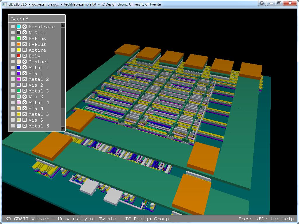
Once the design passes timing sign-off and physical verification, the layout is exported in GDSII format. GDSII is a binary format that represents the layout as a hierarchical collection of polygons on named layers. Each layer in the GDSII file corresponds to a physical layer in the manufacturing process: gate polysilicon, first metal, second metal, via layers, and so on. The foundry uses the GDSII data to generate the photolithographic masks that pattern each layer during fabrication.
The GDSII file is the terminal artifact of the design process. Everything that was designed, verified, and optimized over the course of the project is encoded in this file. The foundry treats it as the authoritative specification of the chip geometry, and what the masks expose onto the wafer is exactly what the GDSII specifies. Errors in the GDSII that were not caught in verification are permanent: the chip will be fabricated with those errors, and fixing them requires another mask set.
Tape-out marks the handoff from design to manufacturing. The fabrication cycle for an advanced node chip typically takes twelve to sixteen weeks. The chip that comes back either works or it does not, and the diagnosis of what went wrong, whether design bugs, physical verification escapes, or manufacturing yield issues, begins from the GDSII and the test results. Getting the GDSII right is the entire objective of everything that came before it.