Summary
| Item | Description |
|---|
| Design | 4-stage ALU (non-pipelined / pipelined / scan-enabled) |
| Purpose | Quantitative study of pipelining, scan insertion, and PD constraints |
| Flow | Yosys → OpenSTA → OpenLane (Sky130) |
| Clock Target | 4.0 ns (post-CTS & signoff closure) |
| Focus | Area, timing, routing, clocking, power trade-offs |
Design Variants
| Variant | Description |
|---|
| Non-Pipelined | Fully combinational datapath |
| Pipelined | 4-stage register boundaries |
| Scan-Pipelined | Pipeline FFs replaced with scan-enabled FFs |
All variants implement identical arithmetic/comparison logic. Only register structure and physical constraints differ.
Synthesis Results (Yosys)
| Metric | Non-Pipe | Pipe | Scan-Pipe |
|---|
| Total Cells | 37 | 50 | 89 |
| Flip-Flops | 0 | 13 | 13 |
| Chip Area ((\mu m^2)) | 538.66 | 891.91 | 1162.04 |
Area Overhead
- Pipelining: +65.6%
- Scan (over pipelined): +30.3%
- Baseline → Scan-Pipelined: +116%
Scan insertion adds ~3 logic gates per flip-flop.
Timing Results (OpenSTA – Baseline Constraints)
| Metric | Non-Pipe | Pipe | Scan-Pipe |
|---|
| Critical Delay (ns) | 1.67 | 0.99 | 1.14 |
| Slack (ns) | 0.33 | 0.88 | 0.74 |
| ( f_{max} ) (MHz) | 598 | 1010 | 877 |
Observations
- Critical path reduction with pipelining: 40.7%
- Frequency improvement: ~1.7×
- Scan overhead: ~150 ps register delay (~13% fmax loss)
- Hold timing clean in all variants
- Scan logic improves minimum delay margins
Pessimistic STA (Interface-Aware Constraints)
Added:
- 50 ps clock uncertainty
- 1.0 ns I/O delays
- Non-zero input slew
| Design | Critical Path | Arrival (ns) | Slack (ns) |
|---|
| Non-Pipe | Input → Output | 2.83 | −1.88 |
| Pipe | Input → Stage-1 FF | 1.54 | +0.27 |
| Scan-Pipe | Input → Scan FF | 1.69 | +0.14 |
Key Results
- Non-pipelined fails timing under realistic constraints
- Pipelining absorbs interface delay
- Scan reduces slack by ~48%, depth unchanged
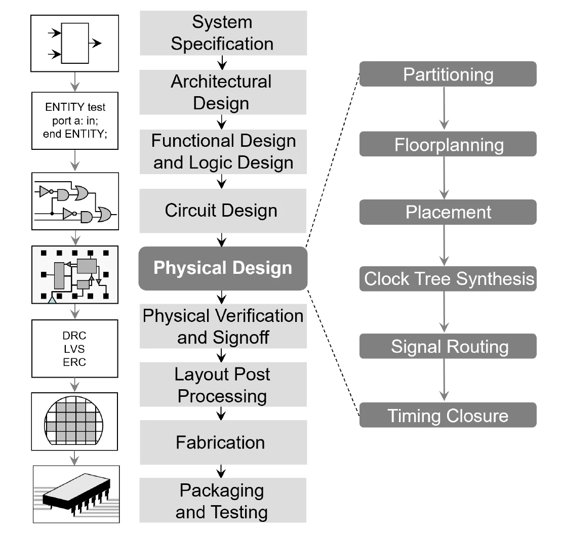
RTL → GDS Physical Design (OpenLane / Sky130)
The scan-pipelined variant was stressed through 10 controlled PD experiments (E1–E10).
Each experiment modified a single dominant physical knob while maintaining timing closure unless specified.
PD Experiment Summary
| Exp | Primary Change | Quantitative Outcome |
|---|
| E1 | Scan baseline, 60% util, CTS skew 0.1 ns | Post-CTS WNS +1.27 ns, power ~8.99e-04 W |
| E2 | Scan removed (control) | Cells 82 → 52, synth WNS +2.22 ns |
| E3 | CTS skew tightened to 0.05 ns | Timing unchanged, ~2× power |
| E4 | FP_CORE_UTIL = 80% | Wirelength 26601 → 26771, WNS ~1.9 ns |
| E5 | Dual scan chains | Clock latency 0.68 → 0.63 ns, power 1.03e-03 W |
| E6 | PL_TARGET_DENSITY = 0.85 | GPL WNS 1.61 → 1.48 ns, DPL recovered |
| E7 | Channelized floorplan | Clock net ~745 → ~788 µm, −70 ps slack |
| E8 | Worst-case IO pinning | Clock net ~1525 µm (~2×) |
| E9 | Pin-architecture fix | Clock net ~703 µm (−54%) |
| E10 | PDN tightening | Total power +21%, switching +58% |
Routing Geometry Evolution
| Metric | E6 | E7 | E8 | E9 | E10 |
|---|
| Clock Net Length (µm) | ~745 | ~788 | 1525 | 703 | ~703 |
| Longest Net (µm) | ~1075 | ~875 | ~1235 | ~1168 | ~1168 |
| scan_out Length (µm) | ~128 | ~329 | ~258 | ~205 | ~205 |
Timing Closure (Post-Route / Signoff)
| Metric | E6 | E7 | E8 | E9 | E10 |
|---|
| Setup WNS (ns) | ~1.45 | ~1.38 | ↓ | ~1.12 | Closed |
| Hold WNS (ns) | ~0.22 | ~0.22 | ~0.22 | ~0.36 | Closed |
| TNS / WNS | 0 / 0 | 0 / 0 | 0 / 0 | 0 / 0 | 0 / 0 |
Power Impact (Signoff, RCX)
| Metric | E9 | E10 |
|---|
| Total Power (W) | 7.48e-04 | 9.06e-04 |
| Switching Power (W) | 2.69e-04 | 4.25e-04 |
| Delta | — | +21% total, +58% switching |
CTS-stage power remained stable; PDN tightening manifested only at signoff.
Consolidated Takeaways
- Pipelining trades ~66% area for ~70% frequency improvement
- Scan insertion adds ~30% area and ~150 ps register delay
- CTS skew tightening affects power, not timing
- Utilization/density ineffective below ~10% real placement density
- Dual scan reduces clock latency but increases routing power
- Floorplan topology affects routing geometry more than timing
- Worst-case IO placement can inflate clock routing by >2×
- Geometry-aware pin restructuring recovers >50% clock routing
- PDN tightening increases signoff switching power by ~58% with timing intact