
CNN Models for CIFAR-10 — Inference Using Verilog, Optimized for Hardware
| Name | CNN For CIFAR10 |
|---|---|
| Description | Implements a light weight CNN in Verilog HDL for better hardware acceleration of image claasification tasks |
| Start | 21 June 2025 |
| Repository | NeVer🔗 |
| Type | Individual |
| Level | Beginner |
| Skills | HDL, Computer Vision, Programming, ML |
| Tools Used | Verilog, Icarus, Python, NumPy |
| Current Status | Ongoing (Active) |
| Progress | - Developed a lightweight CNN [Conv2D×2 + MaxPool]×3 → GAP → Dense(10) for CIFAR-10 Image Classification (32x32RGB) using both IEEE 754 floating-point and Q1.31, Q1.15, Q1.7, and Q1.3 fixed-point arithmetic, achieving 84% accuracy in both implementations (Py ~85% | FP ~84% | Q31 ~84% | Q15 ~84% | Q7 ~82% | Q3 ~65%) |
| Next Steps | - Optimise it for hw inference |
Model Architectures
MODEL_ARCH_1
[ (Conv2D → BN)×2 → MaxPool → Dropout(0.3) ]
→ [ (Conv2D → BN)×2 → MaxPool → Dropout(0.4) ]
→ [ (Conv2D → BN)×2 → MaxPool → Dropout(0.5) ]
→ Flatten → Dense(512) → BN → Dropout(0.5) → Dense(10, softmax)
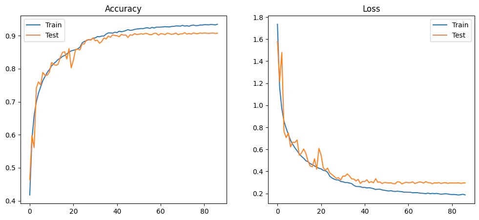
- Number of Parameters:
3,251,018 - Test Accuracy:
90.91%
MODEL_ARCH_2
[ (Conv2D(32) → BN)×2 → MaxPool → Dropout(0.25) ]
→ [ (Conv2D(64) → BN)×2 → MaxPool → Dropout(0.35) ]
→ [ (Conv2D(128) → BN)×2 → MaxPool → Dropout(0.4) ]
→ Flatten → Dense(256) → BN → Dropout(0.5) → Dense(10, softmax)
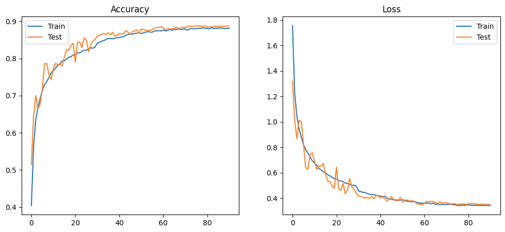
- Number of Parameters:
815,530 - Test Accuracy:
88.84%
MODEL_ARCH_3
[ Conv2D(32)×2 → MaxPool ]
→ [ Conv2D(64)×2 → MaxPool ]
→ [ Conv2D(96) → MaxPool ]
→ Flatten → Dense(256) → Dense(10, softmax)
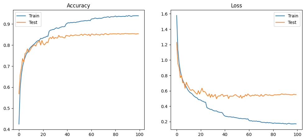
- Number of Parameters:
517,002 - Test Accuracy:
85.53%
MODEL_ARCH_4
[ Conv2D(16)×2 → MaxPool ]
→ [ Conv2D(32)×2 → MaxPool ]
→ [ Conv2D(64)×2 → MaxPool ]
→ GAP → Dense(10, softmax)
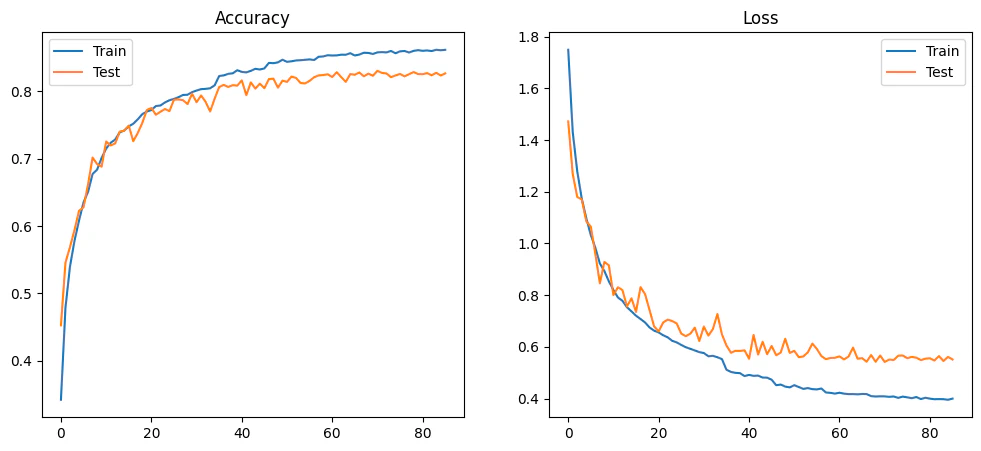
- Number of Parameters:
72,730 - Test Accuracy:
83.05%
Model Architecture Summary
| Model ID | Number of Parameters | Test Accuracy (%) | Model Size (MB) |
|---|---|---|---|
| MODEL_ARCH_1 | 3,251,018 | 90.91 | 12.40 |
| MODEL_ARCH_2 | 815,530 | 88.84 | 3.11 |
| MODEL_ARCH_3 | 517,002 | 85.53 | 1.97 |
| MODEL_ARCH_4 | 72,730 | 83.05 | 0.28 |
Model size calculated assuming 32-bit floating-point weights (
params × 4 bytes ÷ 1024²).
Verilog Inference Q-Point Results
All results are based on a test set of 100 images (10 from each class). The local test accuracy is therefore considered equal to the number of correct predictions out of 100.
All evaluations use the final model [MODEL_ARCH_4] listed in the table above.
| Format | Python Accuracy (%) | Verilog Accuracy (%) | Notes |
|---|---|---|---|
Float32 (Python) vs Float64 IEEE-754 (Verilog real) | 85 | 84 | Verilog used double precision; the minor accuracy difference is not due to precision loss |
| Q1.31 | 84 | 84 | High-precision fixed-point; results match exactly |
| Q1.15 | 84 | 84 | 16-bit fixed-point; results match exactly |
| Q1.7 | 82 | ~82 | Moderate precision; Verilog value estimated from Python result |
| Q1.3 | 65 | ~65 | Low precision; Verilog value estimated from Python result |
YOSYS SYNTHESIS STATS (ONLY 1ST CONV)
   Number of wires:                181
   Number of wire bits:           2514
   Number of public wires:          39
   Number of public wire bits:     422
   Number of memories:               0
   Number of memory bits:            0
   Number of processes:              0
   Number of cells:                165
     $add                           16
     $adff                           5
     $adffe                         14
     $dffe                           5
     $eq                            12
     $ge                             3
     $logic_not                      2
     $logic_or                       3
     $lt                             9
     $mul                            6
     $mux                           41
     $ne                            13
     $neg                            2
     $not                            3
     $pmux                          11
     $reduce_and                    12
     $reduce_bool                    5
     $reduce_or                      1
     $sub                            2


1 modules:
  conv2d_mem
Module Definition:
conv2d_mem- Parameters:
WIDTH,HEIGHT,CHANNELS,FILTERS,K,PAD,BIAS_MODE_POST_ADD. - Ports:
clk,rst,start,done, memory interfaces, andout_dataoutput stream.
- Parameters:
Image ROM interface
image_addr,image_addr_valid,image_addr_ready→ control signals for address request.image_r_data,image_g_data,image_b_data,image_data_valid→ pixel data from memory.image_data_ready→ handshake back to memory.
Kernel ROM interface
kernel_addr,kernel_addr_valid,kernel_addr_ready→ kernel coefficient fetch.kernel_data,kernel_data_valid,kernel_data_ready→ coefficient value transfer.
Bias ROM interface
bias_addr,bias_addr_valid,bias_addr_ready→ bias fetch.bias_data,bias_data_valid,bias_data_ready→ bias value transfer.
Output stream
out_data(32-bit convolution output),out_valid(valid strobe).
Counters and indices
f= filter index,i= row index,j= column index.m,n,c= kernel indices (row, col, channel).in_x,in_y= input coordinates for convolution.kernel_row= computed index for kernel access.
Datapath registers
accum(64-bit accumulator),kernel_mul(48-bit multiply result).out_int,out_int_relu→ final processed outputs.pix_signed,kern16,bias16→ signed extensions of input, kernel, bias.- Latched memory outputs:
image_r_q,image_g_q,image_b_q,kernel_q,bias_q.
FSM (Finite State Machine)
stateregister (6 bits).Localparams define FSM states:
S_IDLE,S_START_FILTER,S_BIAS_REQ,S_BIAS_WAIT,S_SETUP_PIXEL,S_MAC_DECIDE,S_IMG_REQ,S_IMG_WAIT,S_KERN_REQ,S_KERN_WAIT,S_MAC_ACCUM,S_PIXEL_DONE,S_NEXT_PIXEL,S_NEXT_FILTER,S_DONE.
Reset logic
- Initializes FSM to
S_IDLE. - Clears counters, output signals, addresses, and accumulator.
- Initializes FSM to
FSM behavior
S_IDLE: Wait forstart.S_START_FILTER/S_BIAS_REQ: Request bias for current filter.S_BIAS_WAIT: Wait for bias to be valid, latch intobias_q.S_SETUP_PIXEL: Reset accumulator, set pixel iteration counters.S_MAC_DECIDE: Calculate input pixel position (with padding check).S_IMG_REQ/S_IMG_WAIT: Fetch image data.S_KERN_REQ/S_KERN_WAIT: Fetch kernel weight.S_MAC_ACCUM: Multiply-accumulate pixel × weight, updateaccum.S_PIXEL_DONE: Apply bias, normalization, ReLU, setout_data.S_NEXT_PIXEL: Iterate overj,ifor next pixel.S_NEXT_FILTER: Increment filter indexf.S_DONE: Assertdoneafter all pixels and filters are computed.
Bias handling
- Controlled by
BIAS_MODE_POST_ADDparameter. - Option for post-addition bias vs scaled bias.
- Controlled by
Output processing
- Converts accumulator to 32-bit (
out_int). - Applies bias.
- Applies ReLU activation (clamp negative to zero).
- Valid output signaled with
out_valid.
- Converts accumulator to 32-bit (
rom_00_conv2d_bias
==== VIEW A: after frontend (before lowering) ==== Number of wires: 16 Number of wire bits: 46 Number of public wires: 9 Number of public wire bits: 22 Number of memories: 1 Number of memory bits: 128 Number of processes: 2 Number of cells: 4 $logic_and 2 $meminit_v2 1 $memrd 1==== VIEW B: after memory -nomap (abstract memories kept) ==== Number of wires: 17 Number of wire bits: 48 Number of public wires: 8 Number of public wire bits: 18 Number of memories: 0 Number of memory bits: 0 Number of processes: 0 Number of cells: 12 $adff 2 $dff 1 $logic_and 2 $mem_v2 1 $mux 6
==== VIEW C: after synth_xilinx (tech-mapped) ==== Number of wires: 19 Number of wire bits: 52 Number of public wires: 8 Number of public wire bits: 18 Number of memories: 0 Number of memory bits: 0 Number of processes: 0 Number of cells: 36 BUFG 1 FDCE 1 FDPE 1 FDRE 6 IBUF 8 LUT3 1 LUT4 8 OBUF 10
rom_00_conv2d_kernel
==== VIEW A: after frontend (before lowering) ==== Number of wires: 16 Number of wire bits: 61 Number of public wires: 9 Number of public wire bits: 32 Number of memories: 1 Number of memory bits: 3456 Number of processes: 2 Number of cells: 4 $logic_and 2 $meminit_v2 1 $memrd 1==== VIEW B: after memory -nomap (abstract memories kept) ==== Number of wires: 17 Number of wire bits: 53 Number of public wires: 8 Number of public wire bits: 23 Number of memories: 0 Number of memory bits: 0 Number of processes: 0 Number of cells: 12 $adff 2 $dff 1 $logic_and 2 $mem_v2 1 $mux 6
==== VIEW C: after synth_xilinx (tech-mapped) ==== Number of wires: 99 Number of wire bits: 186 Number of public wires: 8 Number of public wire bits: 23 Number of memories: 0 Number of memory bits: 0 Number of processes: 0 Number of cells: 142 BUFG 1 FDCE 1 FDPE 1 FDRE 8 IBUF 13 LUT2 4 LUT3 1 LUT4 2 LUT5 1 LUT6 62 MUXF7 30 MUXF8 8 OBUF 10
image_b_rom
==== VIEW A: after frontend (before lowering) ==== Number of wires: 17 Number of wire bits: 65 Number of public wires: 9 Number of public wire bits: 34 Number of memories: 1 Number of memory bits: 8192 Number of processes: 2 Number of cells: 5 $logic_and 2 $logic_not 1 $meminit_v2 1 $memrd 1==== VIEW B: after memory -nomap (abstract memories kept) ==== Number of wires: 22 Number of wire bits: 86 Number of public wires: 9 Number of public wire bits: 34 Number of memories: 0 Number of memory bits: 0 Number of processes: 0 Number of cells: 17 $dff 4 $logic_and 2 $logic_not 1 $mem_v2 1 $mux 9
==== VIEW C: after synth_xilinx (tech-mapped) ==== Number of wires: 243 Number of wire bits: 504 Number of public wires: 9 Number of public wire bits: 34 Number of memories: 0 Number of memory bits: 0 Number of processes: 0 Number of cells: 360 BUFG 1 FDRE 28 IBUF 14 LUT2 5 LUT3 7 LUT4 6 LUT5 23 LUT6 160 MUXF7 86 MUXF8 20 OBUF 10
Bias ROM: rom_00_conv2d_bias
Views
- VIEW A (Frontend) – memory still modeled as abstract
memwith initialization. - VIEW B (After memory -nomap) – abstract memory removed, lowered into registers + logic.
- VIEW C (After synth_xilinx) – mapped to FPGA primitives (LUTs, FFs, buffers).
- VIEW A (Frontend) – memory still modeled as abstract
Module Definition:
rom_00_conv2d_bias- A small ROM that stores bias values for convolution filters.
- Single-port memory with initialization (
$meminit_v2).
Resource breakdown
VIEW A:
- 1 memory, 128 bits total.
- 2 processes (for initialization and read).
- Simple logic (
$logic_and,$memrd).
VIEW B:
- Memory flattened → 0 memories, instead implemented as FFs + MUX network.
- 12 cells total (2
$adff, 1$dff, 6$mux).
VIEW C:
Fully mapped to FPGA primitives.
36 cells total:
- Sequential logic: 1
FDCE, 1FDPE, 6FDRE(flip-flops). - Combinational logic: LUT3, LUT4 for addressing.
- I/O: 8
IBUF, 10OBUF. - Clocking: 1
BUFG.
- Sequential logic: 1
Summary: The bias ROM is small (128-bit storage), flattened into a few LUTs + registers. It’s essentially a lookup table of per-filter biases, fetched during convolution setup.
Kernel ROM: rom_00_conv2d_kernel
Views
- VIEW A (Frontend) – large memory still intact.
- VIEW B (After memory -nomap) – memory lowered into muxes + registers.
- VIEW C (After synth_xilinx) – mapped into FPGA LUTs, MUXF7/F8 cascade for wide ROM.
Module Definition:
rom_00_conv2d_kernel- Stores kernel weights for convolution (coefficients).
- Much larger than bias ROM: 3456 bits total.
Resource breakdown
VIEW A:
- 1 memory (3456 bits).
- 2 processes, 4 cells.
VIEW B:
- Memory lowered → muxes + FFs.
- 12 cells total (same pattern as bias: 2
$adff, 1$dff, 6$mux).
VIEW C:
Large expansion into 142 FPGA cells.
Breakdown:
- Sequential logic: 1
FDCE, 1FDPE, 8FDRE. - Combinational logic: 62
LUT6, plus smaller LUTs (LUT2, LUT3, LUT4, LUT5). - Wide mux structures: 30
MUXF7, 8MUXF8(used to build large ROM). - I/O: 13
IBUF, 10OBUF. - Clocking: 1
BUFG.
- Sequential logic: 1
Summary: The kernel ROM is significantly larger than the bias ROM (3456 vs 128 bits). After mapping, it consumes many LUT6s and cascaded multiplexers (MUXF7/MUXF8), which is typical for FPGA ROM inference. This block dominates the logic footprint compared to bias.
Blue Channel ROM: image_b_rom
Views
- VIEW A (Frontend) – memory modeled as abstract
$memwith initialization. - VIEW B (After memory -nomap) – memory lowered into registers and combinational logic.
- VIEW C (After synth_xilinx) – mapped to FPGA primitives (LUTs, FFs, buffers).
- VIEW A (Frontend) – memory modeled as abstract
Module Definition:
image_b_rom- Stores the blue channel pixel values for an image block.
- Single-port memory initialized via
$meminit_v2.
Resource breakdown
VIEW A:
- 1 memory, 8192 bits total.
- 2 processes (initialization and read).
- Simple logic:
$logic_and,$logic_not,$memrd. - Total 5 cells.
VIEW B:
Memory flattened → 0 memories, replaced by flip-flops + mux network.
Total 17 cells:
- 4
$dff(flip-flops for state storage) - 2
$logic_and, 1$logic_not - 1
$mem_v2 - 9
$mux(address/data selection)
- 4
VIEW C:
Fully mapped to FPGA primitives.
Total 360 cells:
- Sequential logic: 28
FDREflip-flops. - Combinational logic: 5
LUT2, 7LUT3, 6LUT4, 23LUT5, 160LUT6. - MUX cascades: 86
MUXF7, 20MUXF8. - I/O: 14
IBUF, 10OBUF. - Clocking: 1
BUFG.
- Sequential logic: 28
Summary:
The blue channel ROM is large (8192 bits) and dominates logic usage after tech mapping. It is fully flattened into LUTs, flip-flops, and cascaded multiplexers to implement read access efficiently. Its structure and resource usage are typical for storing image pixel data in FPGA designs.
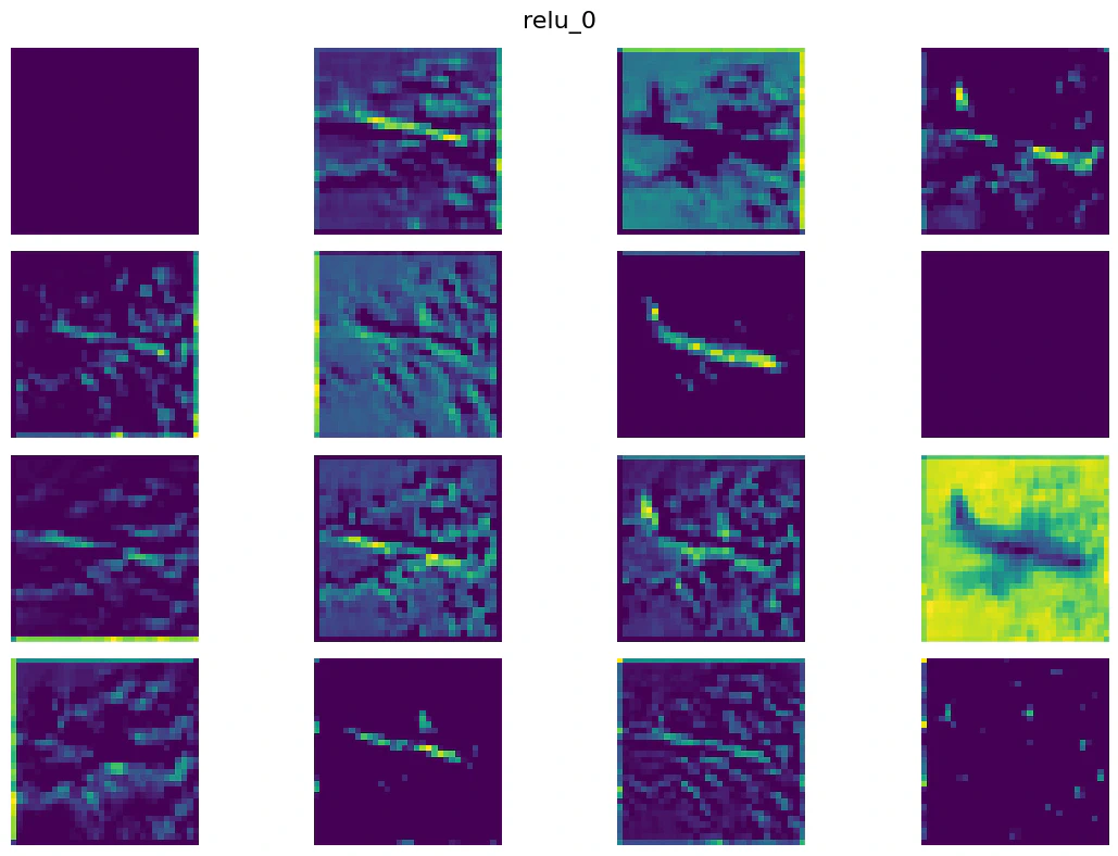
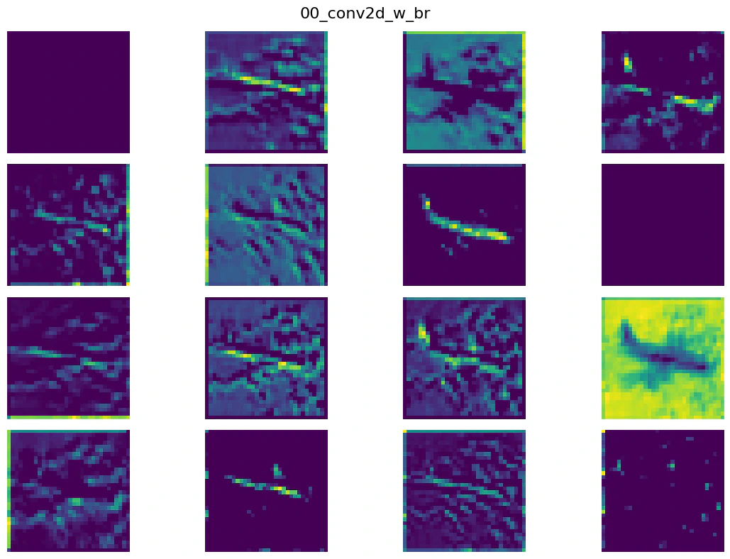
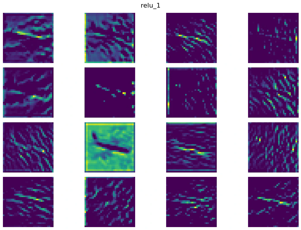
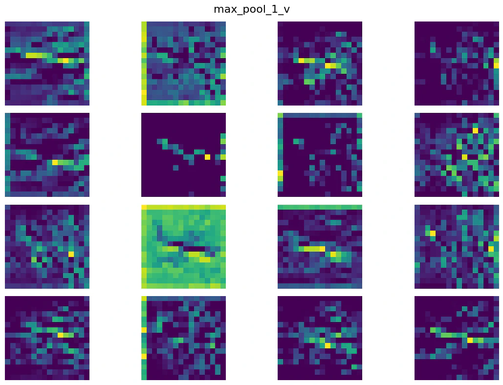
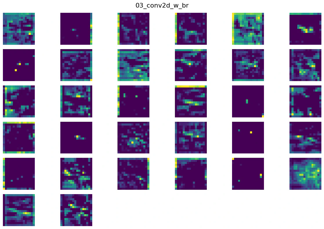
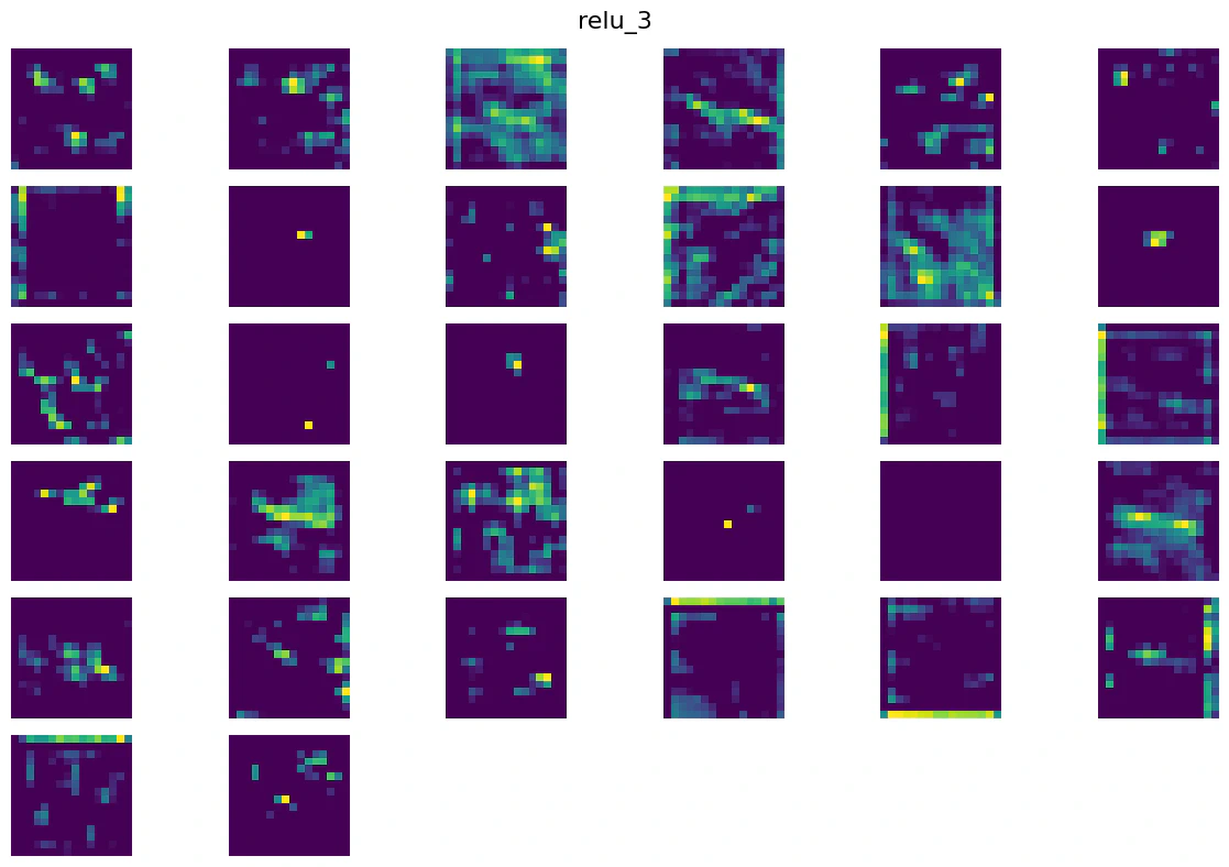
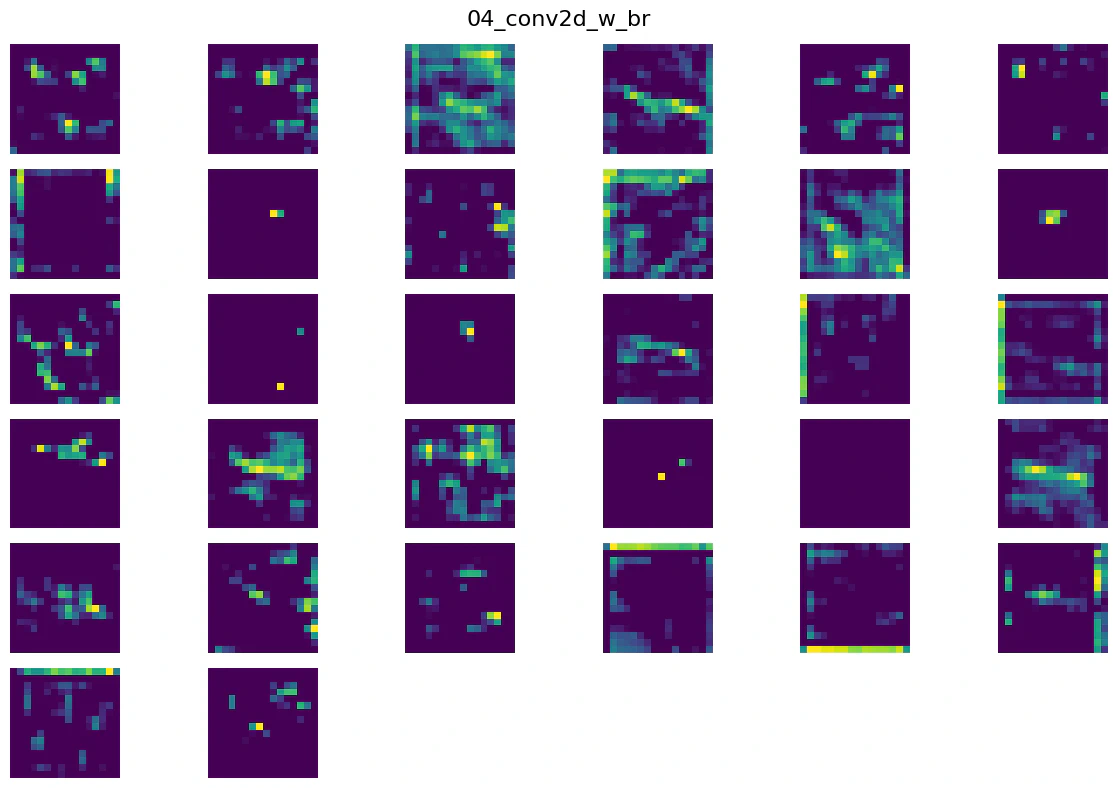
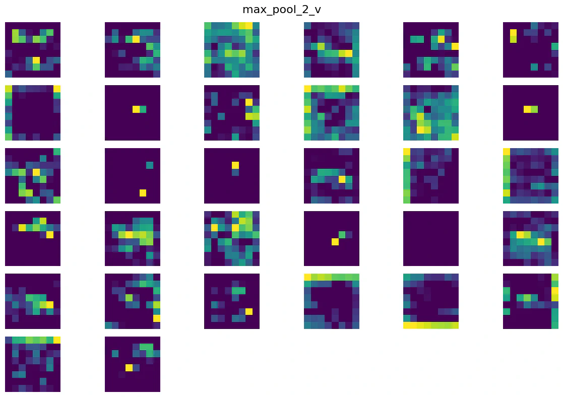
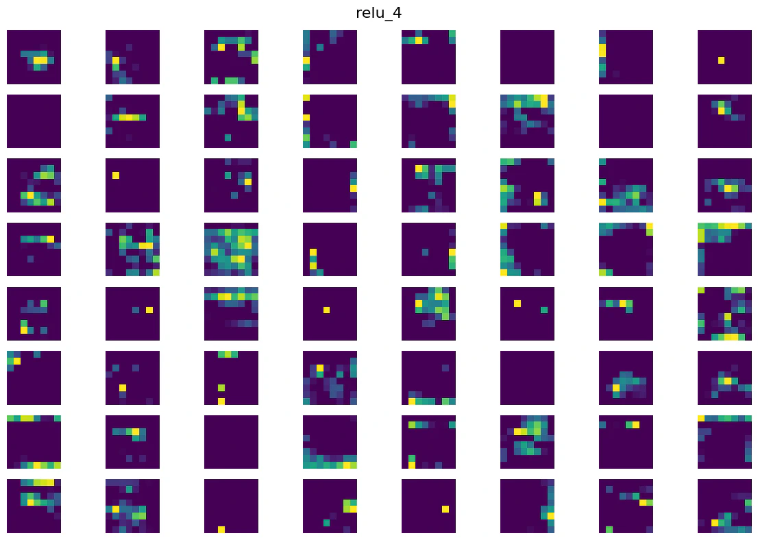
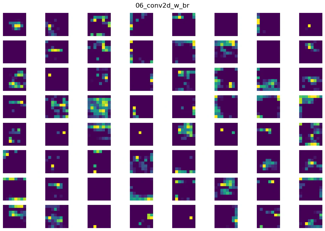
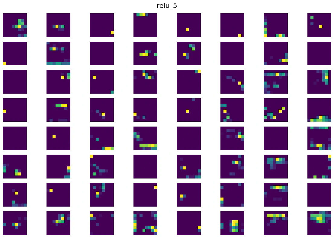
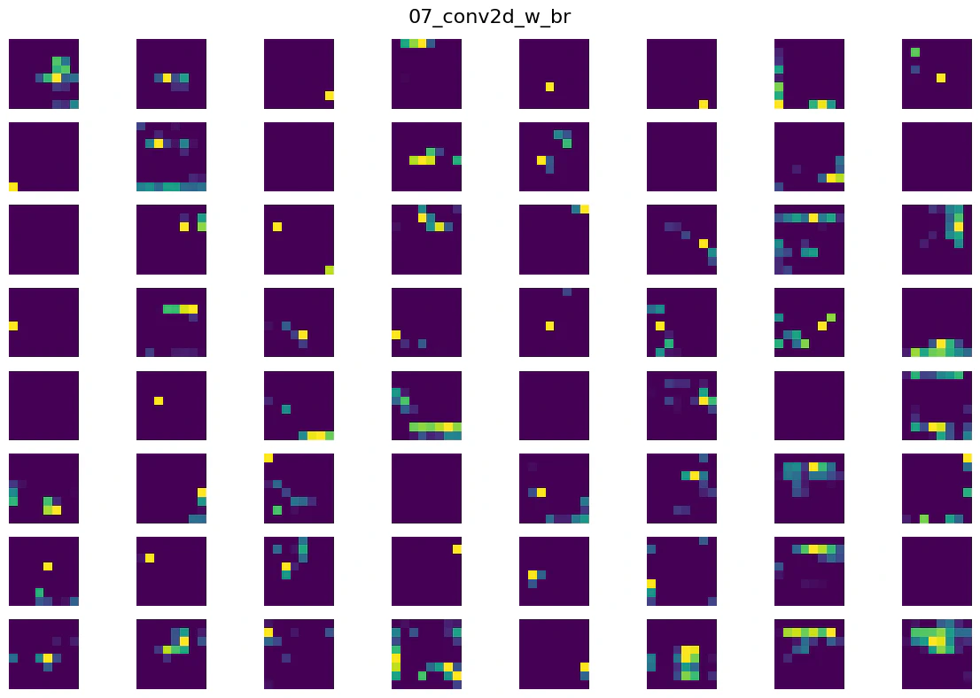
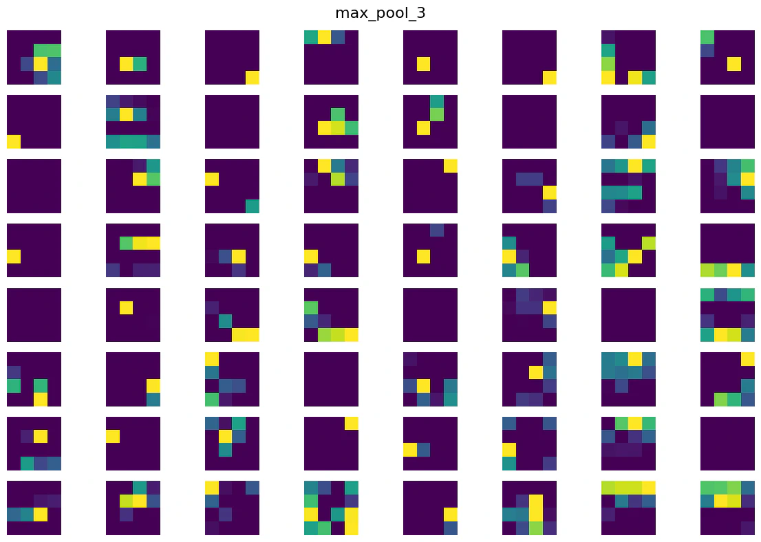
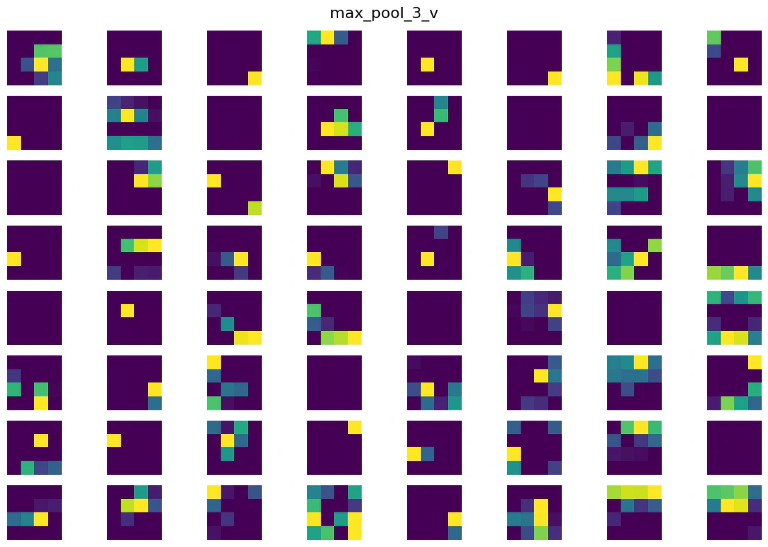
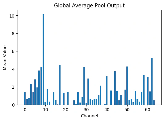
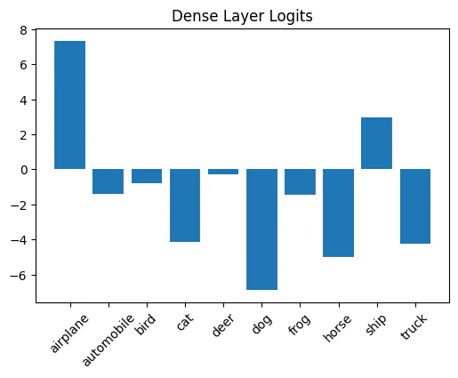
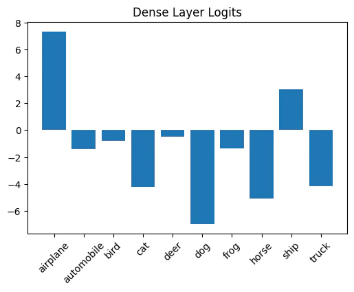
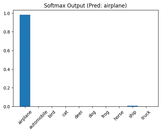
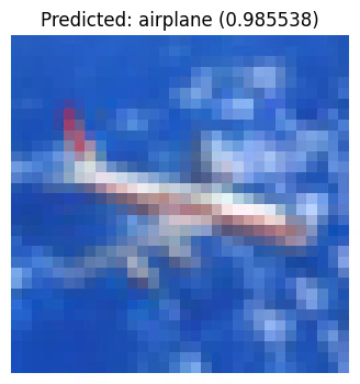
VISUAL COMPARISON FOR PYTHON AND VERILOG
| Python | Verilog |
|---|---|
 |  |
 |  |
 |  |
 |  |
 |  |
 |  |
 |  |
 |  |
 |  |
 |  |
 |  |
 |  |
 |  |
 |  |