
I2C Protocol Verilog Implementation using FSM

| Name | I2C Protocol |
|---|---|
| Description | Verilog Implementation of I2C Protocol using Finite State Machine (FSM) design |
| Start | 06 Nov 2024 |
| Repository | I2CV🔗 |
| Type | Individual |
| Level | Beginner |
| Skills | HDL, Protocols, Programming |
| Tools Used | Verilog, Icarus, Xilinx |
| Current Status | On Hold |
This project implements the I2C protocol in Verilog with various versions and configurations. Below is a summary of each version:
v1.0.2 - Simple Master-Slave (No Clock Stretching)
- Description: This version implements a simple I2C protocol with one master and one slave device. It does not support clock stretching.
- Features:
- Basic I2C communication between a single master and slave.
- No handling of clock stretching; both master and slave devices operate with the same clock frequency.
- NACK will be raised indicating that the given address for slave is wrong.
v2.0.3 - Clock Stretching with Fixed Master Delay
- Description: This version adds support for clock stretching. The master introduces a fixed delay after sending each data frame, and the SCL line will be held low (clock stretching) while waiting for the slave.
- Features:
- Clock stretching is supported for managing communication timing.
- The master introduces a fixed delay to simulate real-world clock stretching scenarios.
v2.0.4 - Clock Stretching with Configurable Master Delay
- Description: This version builds on v2.0.3 by adding a configurable delay from the testbench. The delay allows adjusting the time period that the SCL line waits, providing greater flexibility.
- Features:
- Configurable master delay, adjustable from the testbench.
- SCL waiting period comparison between the master and slave devices.
- Enhanced clock stretching handling with configurable delays.
v3.0.1 - Multi-Slave Single Master Configuration
- Description: This version introduces a configuration with a single master and multiple slave devices. The master can communicate with any of the slaves, supporting multi-slave communication.
- Features:
- One master can communicate with multiple slaves.
- The master can address and select any slave for communication.
- Basic multi-slave handling without clock stretching.
v3.1.1 - Multi-Slave Multi-Master Configuration
- Description: The latest version supports a multi-master, multi-slave configuration, where both the master and slaves can initiate communication. It adds complexity to handle multiple devices that can take control of the bus.
- Features:
- Multiple masters can communicate with multiple slaves.
- Advanced bus arbitration is implemented to handle multiple masters trying to access the bus at the same time.
- Suitable for complex systems requiring both multiple masters and multiple slaves.
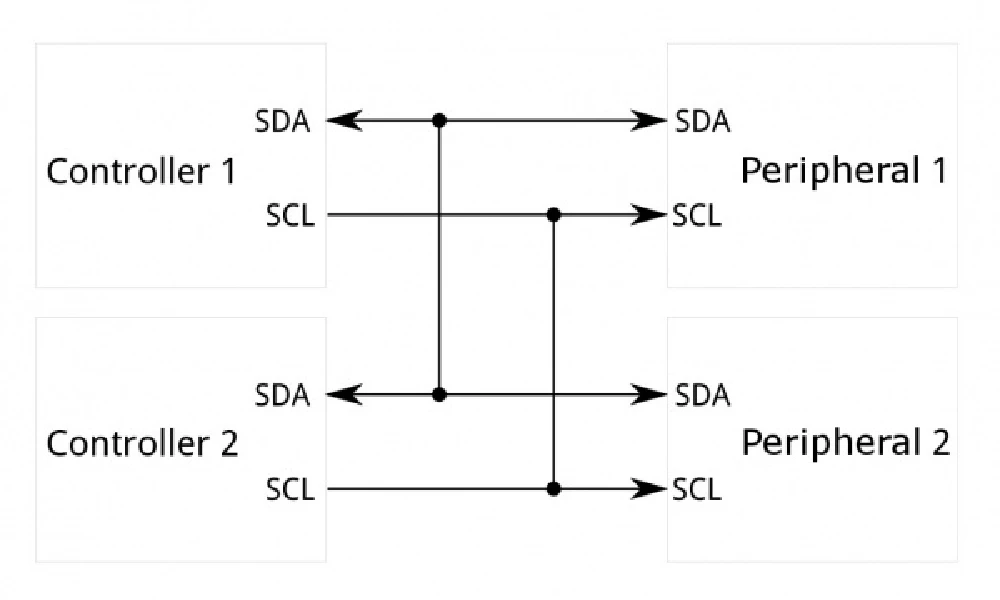
I2C combines the strengths of both UART and SPI. It operates using just two wires, like asynchronous serial, yet supports communication with up to 1,008 peripheral devices. Unlike SPI, I2C accommodates multi-controller systems, allowing more than one controller to communicate with all peripheral devices on the bus (although the controllers must take turns using the bus lines).
I2C data rates fall between those of asynchronous serial and SPI, with most devices communicating at 100 kHz or 400 kHz. While there is some overhead—requiring one additional acknowledgment (ACK/NACK) bit for every 8 bits of data transmitted—I2C remains efficient. Although implementing I2C requires more complex hardware than SPI, it is still simpler than asynchronous serial and can be easily realized in software.
Physical layer
Two-Wire Communication
An I2C system utilizes two shared communication lines for all devices on the bus. These two lines facilitate bidirectional, half-duplex communication. I2C supports multiple controllers and multiple target devices, making it a flexible choice for various applications. It is essential to use pull-up resistors on both of these lines to ensure proper operation. Fig 2.4{reference-type=“ref” reference=“fig:i2c_implementation”} shows a typical implementation of the I2C physical layer.
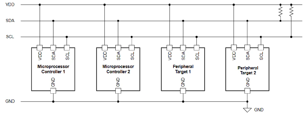
One of the main reasons that I2C is a widely adopted protocol is due to its requirement of only two lines for communication. The first line, SCL, is the serial clock line, primarily controlled by the controller device. SCL is responsible for synchronously clocking data in or out of the target device. The second line, SDA, is the serial data line, used to transmit data to or from the target devices. For instance, a controller device can send configuration data and output codes to a target digital-to-analog converter (DAC), or a target analog-to-digital converter (ADC) can send conversion data back to the controller device.
I2C operates as a half-duplex communication protocol, meaning that only one controller or target device can send data on the bus at any given time. In contrast, the Serial Peripheral Interface (SPI) is a full-duplex protocol that allows data to be sent and received simultaneously, requiring four lines for communication: two data lines for sending and receiving data, along with a serial clock and a unique SPI chip select line to select the device for communication.
An I2C controller device initiates and terminates communication, which eliminates potential issues related to bus contention. Communication with a target device is established through a unique address on the bus, allowing multiple controllers and multiple target devices to coexist on the I2C bus.
The SDA and SCL lines have an open-drain connection to all devices on the bus, necessitating a pull-up resistor connected to a common voltage supply.
Open-Drain Connection
The open-drain connections are employed on both the SDA and SCL lines and are linked to an NMOS transistor. This open-drain configuration manages the I2C communication line by either pulling the line low or allowing it to rise to a high state. The term "open-drain" refers to the NMOS bus connection when the NMOS is turned OFF. Figure 2.5{reference-type=“ref” reference=“fig:open_drain_connection”} illustrates the open-drain connection when the NMOS is turned ON.
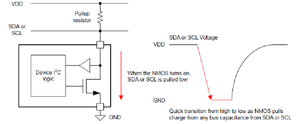
To establish the voltage level of the SDA or SCL line, the NMOS transistor is either switched ON or OFF. When the NMOS is ON, it allows current to flow through the resistor to ground, effectively pulling the open-drain line low. This transition from high to low is typically rapid, as the NMOS quickly discharges any capacitance on the SDA or SCL lines.
When the NMOS turns OFF, the device ceases to pull current, and the pull-up resistor subsequently raises the SDA or SCL line back to VDD. Figure 2.6{reference-type=“ref” reference=“fig:open_drain_off”} shows the open-drain line when the NMOS is turned OFF, illustrating how the pull-up resistor brings the line high.
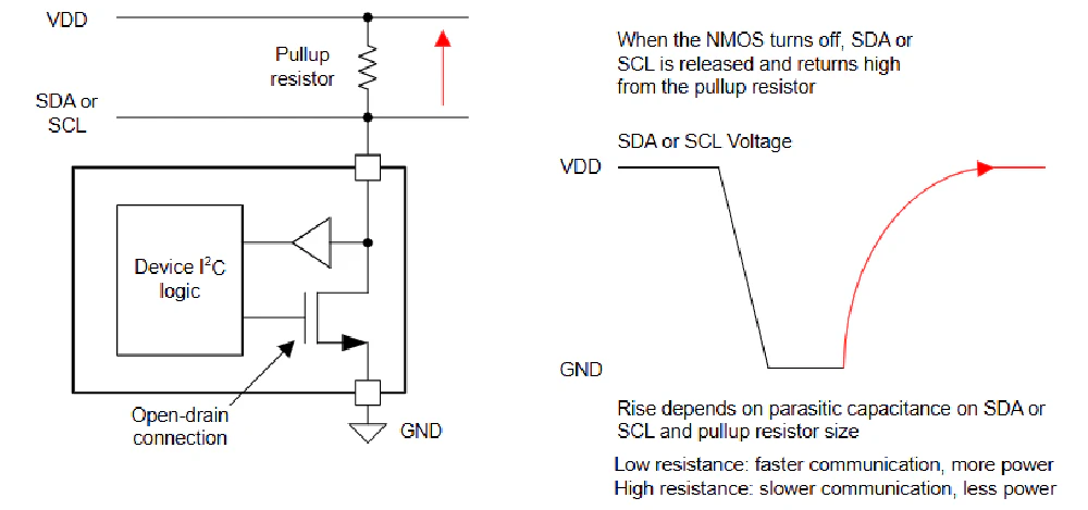
The transition of the open-drain line to a high state is slower because the line is pulled up against the bus capacitance, rather than being actively driven high.
I2C Protocol
Communication over I2C requires a specific signaling protocol to ensure that devices on the bus recognize valid I2C transmissions. While this process is more intricate than UART or SPI, most I2C-compatible devices handle the finer protocol details internally, allowing developers to focus primarily on data exchange.
SDA and SCL Lines: The I2C bus operates with two main lines: SDA (Serial Data Line) and SCL (Serial Clock Line). Data is transmitted over the SDA line in sync with clock pulses on the SCL line. Generally, data is placed on SDA when SCL is low, and devices sample this data when SCL goes high. If needed, multiple internal registers may control data handling, especially in complex devices.
Protocol Components:
1. Start Condition: To initiate communication, the controller sets SCL high and then pulls SDA low. This signals all peripheral devices on the bus that a transmission is starting. In cases where multiple controllers attempt to start communication simultaneously, the first device to pull SDA low gains control. If necessary, the controller can issue repeated start conditions to maintain bus control without releasing it.
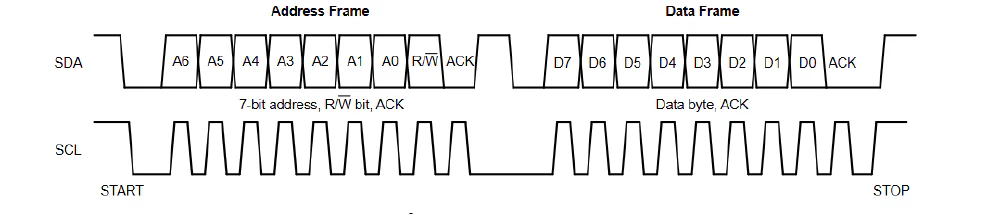
2. Address Frame: Every I2C transmission begins with an address frame to specify the target peripheral. This frame consists of a 7-bit address, sent MSB (most significant bit) first, followed by a R/W bit indicating the operation type (read or write).
After this, the 9th bit, known as the ACK/NACK bit, is used by the receiving device to confirm reception. If the device pulls SDA low before the 9th clock pulse (ACK), communication continues. If not (NACK), it indicates either unrecognized data or an issue in reception, prompting the controller to decide the next steps.
3. Data Frames: Following the address frame, one or more data frames are sent over the SDA line. Each data frame is 8 bits, and data is transferred from the controller to the peripheral or vice versa, based on the R/W bit in the address frame.
Many peripheral devices have auto-incrementing internal registers, enabling data to continue from consecutive registers without the need to re-specify the register address.
4. Stop Condition: The controller ends communication by generating a stop condition. This is done by transitioning SDA from low to high after a high-to-low transition on SCL, with SCL held high during the stop sequence. To avoid false stop conditions, the value on SDA should not change while SCL is high during regular data transmission.
The I2C protocol divides communication into structured frames. Each communication sequence begins with a START condition, initiated by the controller, followed by an address frame and then one or more data frames. Every frame also includes an acknowledgment (ACK) bit, signaling that the frame has been received successfully by the intended device. Figure 3-3 illustrates the structure of two I2C communication frames, showing both address and data frames in detail.
In an I2C transaction, the controller first sends a START condition by pulling the SDA line low, followed by the SCL line. This sequence asserts control over the bus, preventing other devices from interfering. Each target device on the I2C bus has a unique 7-bit address, allowing the controller to specify which target device it intends to communicate with.
Once the address is set on SDA while SCL acts as the clock, the 8th bit (R/W bit) indicates the intended operation type: read (1) or write (0). This initial address and R/W bit are followed by an ACK bit, sent by the target device to confirm receipt. If the target device receives the address successfully, it pulls SDA low during the next SCL pulse, signaling an ACK. If no device acknowledges, the line remains high, signaling a NACK.
After the address frame, one or more data frames follow. Each data frame contains 8 bits of data, which are acknowledged (ACK) in the 9th bit. If the data frame is a write operation, the target device pulls SDA low to confirm data receipt. For read operations, the controller pulls SDA low to acknowledge receipt of the data. The presence or absence of the ACK is essential for troubleshooting, as a missing ACK may indicate an addressing error or transmission failure.
Finally, the communication ends with a STOP condition, where the controller releases SCL first, followed by SDA. This action releases the I2C bus for other devices to use, completing the communication cycle.
This structured protocol allows for the transmission of multiple bytes within one communication sequence. In cases where a target device has multiple internal registers, a write operation can specify the register to read or write data to, enhancing flexibility and enabling complex data transactions.
Module Specifications
MASTER MODULE
CODE
This module enables communication with I2C-compatible devices through the I2C protocol by implementing the necessary operations to generate I2C signals and manage data transfer. Let’s break down each section of the code:
Module Declaration
The code begins with the module declaration:
module i2c_master(
    input wire clk,               // System clock
    input wire rst,               // Synchronous reset
    input wire [6:0] addr,        // 7-bit I2C address
    input wire [7:0] data_in,     // Data to be transmitted
    input wire enable,            // Enable signal to start I2C transaction
    input wire rw,                // Read/Write control (0 = Write, 1 = Read)
    output reg [7:0] data_out,    // Data received from I2C
    output wire ready,            // Ready signal when module is idle
    inout i2c_sda,                // I2C data line (SDA)
    inout wire i2c_scl            // I2C clock line (SCL)
);
This module contains inputs for the system clock (clk), reset (rst),
I2C address (addr), data to be sent (data_in), an enable signal
(enable), and a Read/Write control (rw). It also provides outputs
for data received (data_out), a ready status signal (ready), and
bidirectional I2C lines, i2c_sda and i2c_scl.
State Machine Definition
The code defines several states representing stages in the I2C transaction:
localparam IDLE = 0;
localparam START = 1;
localparam ADDRESS = 2;
localparam READ_ACK = 3;
localparam WRITE_DATA = 4;
localparam WRITE_ACK = 5;
localparam READ_DATA = 6;
localparam READ_ACK2 = 7;
localparam STOP = 8;
Each localparam corresponds to a state in the Finite State Machine
(FSM), controlling the I2C protocol flow, including start, address
transmission, acknowledgment (ACK) reception, data transfer, and stop
condition generation.
Clock Divider
To generate a slower clock for the I2C operations, a clock divider is implemented:
always @(posedge clk) begin
    if (counter2 == (DIVIDE_BY / 2) - 1) begin
        i2c_clk <= ~i2c_clk;
        counter2 <= 0;
    end else counter2 <= counter2 + 1;
end
This block toggles i2c_clk at a lower frequency than the system clock,
clk, using a counter counter2 with a division factor defined by
DIVIDE_BY.
SDA and SCL Control
To control the i2c_sda and i2c_scl lines based on the module’s
state:
assign ready = ((rst == 0) && (state == IDLE)) ? 1 : 0;
assign i2c_scl = (i2c_scl_enable == 0) ? 1 : i2c_clk;
assign i2c_sda = (write_enable == 1) ? sda_out : 'bz;
readyis high when the reset is inactive and the state isIDLE.i2c_sclis either high (idle state) or follows the dividedi2c_clksignal.i2c_sdaoutputs the value ofsda_outwhenwrite_enableis active. Whenwrite_enableis inactive,i2c_sdagoes to high-impedance (’bz) for reading data.
Finite State Machine (FSM)
The FSM controls the I2C communication process, progressing through states based on the I2C protocol requirements:
always @(posedge i2c_clk or posedge rst) begin
    if (rst == 1) begin
        state <= IDLE;
    end else begin
        case (state)
            IDLE: begin
                if (enable) begin
                    state <= START;
                    saved_addr <= {addr, rw};
                    saved_data <= data_in;
                end
            end
            START: begin
                counter <= 7;
                state <= ADDRESS;
            end
            ...
            STOP: begin
                state <= IDLE;
            end
        endcase
    end
end
Each state corresponds to an I2C operation:
IDLE: Waits forenablesignal to initiate communication.START: Prepares a start condition by assertingsda_outlow.ADDRESS: Sends the address and R/W bit.READ_ACKandREAD_ACK2: Verifies acknowledgment (ACK) from the slave.WRITE_DATAandWRITE_ACK: Transfers data to the slave and waits for ACK.READ_DATA: Receives data from the slave.STOP: Generates a stop condition and returns toIDLE.
SDA Output Logic
The logic for controlling the i2c_sda line, depending on the FSM
state, is implemented as follows:
always @(negedge i2c_clk or posedge rst) begin
    if (rst == 1) begin
        write_enable <= 1;
        sda_out <= 1;
    end else begin
        case (state)
            START: begin
                write_enable <= 1;
                sda_out <= 0;
            end
            ADDRESS: begin
                sda_out <= saved_addr[counter];
            end
            ...
            STOP: begin
                write_enable <= 1;
                sda_out <= 1;
            end
        endcase
    end
end
In the
STARTstate,sda_outgoes low to generate a start condition.In the
ADDRESSandWRITE_DATAstates,sda_outsends the bits ofsaved_addrorsaved_data.In
STOP,sda_outgoes high to signify the end of the transmission.
This Verilog module effectively implements an I2C Master communication
sequence by controlling the i2c_sda and i2c_scl lines according to
the I2C protocol.
SLAVE MODULE
CODE
I2C Slave Module implements the core logic for an I2C slave device capable of receiving and transmitting data over the I2C protocol. Let’s break down the components of the code and their functionality:
Module Declaration
The module begins with the declaration of inputs and outputs:
module i2c_slave(
    input [6:0] addr_in,   // Dynamic address input for I2C slave
    inout sda,             // I2C data line (SDA)
    inout scl              // I2C clock line (SCL)
);
The inputs include a 7-bit address (addr_in) for the slave device,
along with the bidirectional sda and scl lines for data and clock
signals respectively.
State Machine Definition
The I2C protocol relies on a finite state machine (FSM) to control the data transfer sequence. The FSM is represented by five states:
localparam READ_ADDR = 0;
localparam SEND_ACK = 1;
localparam READ_DATA = 2;
localparam WRITE_DATA = 3;
localparam SEND_ACK2 = 4;
Each state corresponds to a particular phase of the I2C communication: -
READ_ADDR: Reads the I2C address and R/W bit. - SEND_ACK: Sends
acknowledgment (ACK) if the address matches. - READ_DATA: Receives
data from the master. - WRITE_DATA: Sends data to the master. -
SEND_ACK2: Sends a second ACK after data reception.
Internal Registers and Signals
Several internal registers and signals are declared to support the
functionality of the I2C slave: - addr holds the slave address and R/W
bit. - counter is used to count bits during transmission. - state
holds the current FSM state. - data_in and data_out store the
incoming and outgoing data, respectively. - sda_out and sda_in
control the data line (SDA). - start flags the detection of the I2C
start condition. - write_enable controls whether the slave can drive
the SDA line.
SDA Line Control
The assignment of the sda line is conditional on the write_enable
signal:
assign sda = (write_enable == 1) ? sda_out : 'bz;
This means that the slave drives the sda line when write_enable is
active, otherwise, the line is in high-impedance state (‘bz).
Start and Stop Condition Detection
The start condition is detected when there is a falling edge on the
sda line while the scl line is high, and the stop condition is
detected when there is a rising edge on the sda line while scl is
high. These conditions trigger transitions in the FSM.
always @(negedge sda) begin
    if ((start == 0) && (scl == 1)) begin
        start <= 1;           // Set start flag
        counter <= 7;         // Initialize bit counter
    end
end

always @(posedge sda) begin
    if ((start == 1) && (scl == 1)) begin
        state <= READ_ADDR;   // Transition to READ_ADDR state
        start <= 0;           // Reset start flag
        write_enable <= 0;    // Disable write
    end
end
These blocks capture the start and stop conditions and manage the FSM transitions accordingly.
FSM Logic for Data Transfer
The FSM operates on the rising edge of the scl signal, progressing
through various states based on the detected conditions:
always @(posedge scl) begin
    if (start == 1) begin
        case(state)
            READ_ADDR: begin
                addr[counter] <= sda;
                if(counter == 0) state <= SEND_ACK;
                else counter <= counter - 1;
            end
            SEND_ACK: begin
                if(addr[7:1] == addr_in) begin
                    counter <= 7;
                    if(addr[0] == 0) begin
                        state <= READ_DATA; // If write mode, move to READ_DATA
                    end else state <= WRITE_DATA; // Else move to WRITE_DATA
                end else state <= READ_ADDR;
            end
            ...
        endcase
    end
end
The state transitions depend on whether the address matches, the R/W
bit, and whether data is being read or written. The SEND_ACK state
sends an acknowledgment if the address is correct, while the READ_DATA
and WRITE_DATA states handle data reception and transmission
respectively.
SDA Output Logic
The logic for controlling the sda output during the FSM states is
defined in the following block:
always @(negedge scl) begin
    case(state)
        READ_ADDR: begin
            write_enable <= 0;            // Disable writing during address read
        end
        SEND_ACK: begin
            sda_out <= (addr[7:1] == addr_in) ? 0 : 1;  // Send ACK (0) or NACK (1)
            write_enable <= 1;
        end
        READ_DATA: begin
            write_enable <= 0;           // Disable writing during data read
        end
        WRITE_DATA: begin
            sda_out <= data_out[counter]; // Output data bit by bit
            write_enable <= 1;
        end
        SEND_ACK2: begin
            sda_out <= 0;                // Send ACK (0) after data reception
            write_enable <= 1;
        end
    endcase
end
Each state manipulates the sda_out signal to either send an
acknowledgment (ACK) or transmit the data bit by bit. The SEND_ACK
state checks the address match and sends either an ACK or NACK. The
WRITE_DATA state sends the data, while the SEND_ACK2 state sends an
ACK after data reception.
Summary
This Verilog code implements a simple I2C Slave module that can handle basic I2C communication. It includes start/stop condition detection, address matching, data reception, and data transmission using an FSM. The module can receive data from the I2C master, send data to it, and properly acknowledge the master at each step in the communication process.
TOP-LEVEL MODULE
CODE
`timescale 1ns / 1ps

// Top module to integrate i2c_master and i2c_slave
// Top module to integrate i2c_master and i2c_slave
module top(
    input wire clk,                 // System clock
    input wire rst,                 // Reset signal
    input wire [6:0] addr,          // 7-bit I2C address for the master to communicate with
    input wire [7:0] data_in,       // Data to be sent from the master to the slave
    input wire enable,              // Enable signal to initiate I2C communication
    input wire rw,                  // Read/Write signal (0 = Write, 1 = Read)
    output wire [7:0] data_out,     // Data received by the master from the slave
    output wire ready,              // Signal indicating the master is ready for a new operation
    inout wire i2c_sda,             // I2C data line (SDA) - bidirectional
    inout wire i2c_scl              // I2C clock line (SCL)
);

    // Internal register to store the address the slave will respond to.
    // This is the fixed address of the slave in this example.
    reg [6:0] slave_address = 7'b0101010;  // Example default slave address

    // Instantiate the I2C slave module
    i2c_slave slave_inst (
        .addr_in(slave_address),   // Provide the fixed slave address to the slave instance
        .sda(i2c_sda),             // Connect the slave's SDA line to the top-level SDA
        .scl(i2c_scl)              // Connect the slave's SCL line to the top-level SCL
    );

    // Instantiate the I2C master module
    i2c_master master_inst (
        .clk(clk),                 // Connect the system clock to the master
        .rst(rst),                 // Connect the reset signal to the master
        .addr(addr),               // Provide the I2C address the master should communicate with
        .data_in(data_in),         // Data to be sent to the slave (if writing)
        .enable(enable),           // Enable signal to start the I2C transaction
        .rw(rw),                   // Read/Write signal (0 = Write, 1 = Read)
        .data_out(data_out),       // Data received from the slave (if reading)
        .ready(ready),             // Master ready signal indicating it's idle or ready for a new transaction
        .i2c_sda(i2c_sda),         // Connect the master's SDA line to the top-level SDA
        .i2c_scl(i2c_scl)          // Connect the master's SCL line to the top-level SCL
    );

endmodule
Explanation
The
topmodule connects an I2C master and slave module on sharedi2c_sdaandi2c_scllines.The
slave_addressregister holds a predefined address used by the slave.The
i2c_slaveandi2c_mastermodules are instantiated and connected to share the I2C lines and control signals.
TESTBENCH MODULE
CODE
`timescale 1ns / 1ps

module i2c_controller_tb();

    // Inputs
    reg clk;                  // System clock
    reg rst;                  // Reset signal
    reg [6:0] addr;           // Address for the master to communicate with
    reg [7:0] data_in;        // Data to be sent from the master to the slave
    reg enable;               // Enable signal to start communication
    reg rw;                   // Read/Write control (0 = Write, 1 = Read)

    // Outputs
    wire [7:0] data_out;      // Data received by the master from the slave
    wire ready;               // Ready signal indicating the master is ready for a new operation

    // Bidirectional wires
    wire i2c_sda;             // I2C data line (SDA) - shared between master and slave
    wire i2c_scl;             // I2C clock line (SCL) - shared between master and slave

    // Instantiate the Top Module (Device Under Test - DUT)
    top uut (
        .clk(clk),           // Connect system clock to DUT
        .rst(rst),           // Connect reset signal to DUT
        .addr(addr),         // Connect address input to DUT
        .data_in(data_in),   // Connect data to be sent by master to DUT
        .enable(enable),     // Connect enable signal to DUT
        .rw(rw),             // Connect read/write control to DUT
        .data_out(data_out), // Receive data read by master from DUT
        .ready(ready),       // Receive ready signal from DUT
        .i2c_sda(i2c_sda),   // Connect bidirectional SDA line
        .i2c_scl(i2c_scl)    // Connect bidirectional SCL line
    );

    // Clock generation
    initial begin
        clk = 0;
        forever #1 clk = ~clk;  // Toggle clock every 1 ns to generate a 2 ns period clock (500 MHz)
    end

    // Test sequence to simulate I2C operations
    initial begin
        // Set up VCD file for waveform dumping
        $dumpfile("i2c_controller_tb.vcd");  // Name of the VCD file for waveform output
        $dumpvars(0, i2c_controller_tb);     // Dump all variables in this module for waveform analysis

        // Initialize Inputs
        rst = 1;           // Assert reset to initialize the system
        enable = 0;        // Initially disable communication
        addr = 7'b0000000; // Set an initial address (not used immediately)
        data_in = 8'b0;    // Set initial data (not used immediately)
        rw = 0;            // Set initial operation to write (0 = Write, 1 = Read)

        // Wait for reset to complete
        #10;
        rst = 0;           // Deassert reset after 10 ns to start normal operation

        // Test Case 1: Write operation with matching address (Expect ACK from slave)
        addr = 7'b0101010;       // Set address to match the slave address
        data_in = 8'b10101010;   // Data to be sent to the slave
        rw = 0;                  // Set operation to write
        enable = 1;              // Assert enable to start the I2C communication
        #20 enable = 0;          // Deassert enable after 20 ns to complete the command

        // Wait and observe response (slave should ACK the address and receive data)
        #100;

        // Test Case 2: Write operation with non-matching address (Expect NACK from slave)
        addr = 7'b1111111;       // Set address to a non-matching address for the slave
        data_in = 8'b11001100;   // Different data to be sent to the slave
        rw = 0;                  // Set operation to write
        enable = 1;              // Assert enable to start the I2C communication
        #20 enable = 0;          // Deassert enable after 20 ns

        // Wait and observe response (slave should NACK the address since it does not match)
        #100;

        // Test Case 3: Read operation with matching address (Expect ACK from slave and read data)
        addr = 7'b0101010;       // Set address to match the slave address
        rw = 1;                  // Set operation to read
        enable = 1;              // Assert enable to start the I2C communication
        #20 enable = 0;          // Deassert enable after 20 ns

        // Wait and observe response (slave should ACK the address and send data to master)
        #100;

        #200
        $finish;  // End the simulation after 200 ns
    end

endmodule
Explanation
i2c_controller_tb: Testbench module for thetopmodule integrating the master-slave I2C communication.A clock signal is generated using a continuous
initialblock.Test cases:
Test Case 1: Matches the slave address, expecting an ACK.
Test Case 2: Uses a non-matching address, expecting a NACK.
Test Case 3: Matches the address and tests a read operation.
At the end of the test cases, the simulation finishes with
$finish.
Results
Test Case 1: Address Match with Write Operation
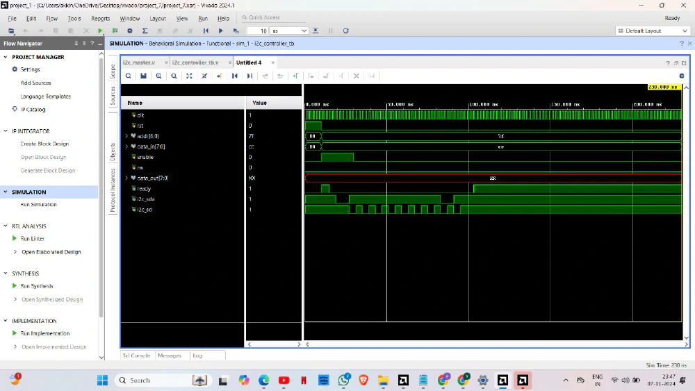
The waveform in this test shows the master sending an address 7’b0101010, which matches the slave’s configured address. Since the address matches, the slave acknowledges the communication by sending an ACK (acknowledgment) signal. After receiving the ACK, the master initiates a write operation, transmitting the data 8’b10101010 to the slave. The enable signal is set to initiate communication and deasserted after a delay, allowing the transmission to complete. The presence of the ACK in this waveform confirms that the address was successfully matched, allowing data transfer.
Test Case 2: Address Mismatch with Write Operation (Expect NACK)
In this test case, the master sends a non-matching address 7’b1111111, which does not correspond to the slave’s preset address. The waveform shows the absence of an acknowledgment signal (NACK) from the slave, indicating that the address verification failed and the data transfer cannot proceed. This NACK response is expected behavior when the slave does not recognize the transmitted address. The enable signal initiates the communication, but with no matching address and no ACK received, data transfer is not established.
Test Case 3: Address Match with Read Operation
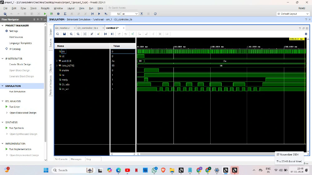
The final waveform demonstrates a read operation with the master sending a matching address 7’b0101010. Upon recognizing the address, the slave responds with an ACK signal, confirming the communication link. Following the acknowledgment, the master initiates a read operation, and the slave provides the preloaded data 8’b11001100 to the master. The enable signal triggers the start of communication and is deasserted after a delay, allowing the master to read the data. This successful transmission and receipt of data verify correct read functionality with an address match.
Challenges and Risk Analysis
Potential Issues and Solutions
In the development of the I2C communication project, I encountered several challenges, starting with the design of basic Verilog modules for both master and slave entities capable of fundamental read and write operations. After an initial review of the I2C protocol from various online resources and Verilog syntax, I designed a preliminary testbench module to simulate and validate the basic functionality.
As the project progressed, I introduced additional functionality, including ACK and NACK flags, to handle incorrect slave addresses and refined the finite state machine (FSM) logic for more reliable state transitions. To make the slave module independent of global configurations, I designed a top-level module that instantiated both the master and slave modules and added an extra layer of address validation.
For synchronization, I implemented clock stretching between address and data frames. This addition worked effectively during address transmission but revealed timing issues during data frame read operations. After extensive troubleshooting, I identified limitations in the initial approach and modified the design accordingly.
I also explored a multi-master, multi-slave configuration, assigning slave addresses in the format 10101XY (with XY values as 00, 01, 10, and 11 for slaves 1 through 4) and a master select line in the testbench to choose the active master. Preloaded data in each slave was structured as 110011XY to streamline read operations. However, unresolved synchronization issues in the multi-master setup led me to scale back to a single-master, single-slave model, excluding clock stretching and multiple nodes. The final design focuses on single-point communication, with code attempts for the multi-master setup included in the project appendix on GitHub.
Risk Management
Several potential risks emerged during the design and integration phases:
Design Complexity: The complexity of the I2C protocol and multi-node configuration posed unforeseen design challenges. A modular testing approach mitigated these risks by allowing iterative refinements.
Timing Issues: Timing mismatches, particularly in multi-master configurations, impacted protocol accuracy. While resolved in the single-master model, this remains an area for future improvement.
FSM Complexity: Introducing ACK/NACK handling increased the complexity of the FSM, raising the potential for state transition errors. Comprehensive simulation and debugging minimized these risks.
In this project, I implemented the clock stretching functionality and addressed timing issues in data frame read operations. Starting with basic I2C modules, I managed the synchronization aspect by incorporating clock stretching between address and data frames, a mechanism crucial for addressing timing issues in the protocol. Despite progress, some discrepancies remain in the data frame during read operations, which are planned for future enhancements.
Additionally, I expanded the basic modules by introducing acknowledgment (ACK) and negative acknowledgment (NACK) flags to handle erroneous addresses. I refined the FSM logic to improve state transitions, address handling, and protocol management complexities. While the initial goal was a multi-master configuration with selectable slave nodes, unresolved timing issues led to a focus on a single-master, single-slave model, effectively capturing the core aspects of I2C communication in the final implementation.
Future Work and Improvements
Suggested Enhancements
Future enhancements to this project could include adding more registers to each slave, allowing for more sophisticated data handling. Additional registers would enable more extensive data storage and retrieval options in each slave device, making the project closer to real-world I2C applications.
Alternative Designs
Exploring alternative FSM architectures could improve the efficiency and stability of the I2C protocol, especially for multi-master configurations. Further, advanced data synchronization techniques, possibly through modified clock stretching or data frame timing adjustments, could address the current timing issues. Replacing the current point-to-point master-slave setup with a robust multi-node configuration, if resolved, could significantly enhance the protocol’s scalability.
Appendices
Verilog Code Listings
The complete Verilog code for the I2C Master module, including support for multi-master/slave configuration and clock stretching, is available in the following GitHub repository:
Repository: https://github.com/Mummanajagadeesh/I2C-protocol-verilog
References
Texas Instruments, A Basic Guide to I2C, Available at: https://www.ti.com/lit/pdf/sbaa565
Prodigy Technoinnovations, I2C Protocol, Available at: https://www.prodigytechno.com/i2c-protocol
SparkFun, I2C Tutorial, Available at: https://learn.sparkfun.com/tutorials/i2c/all
Class Lectures, Verilog Code Syntax
Most images in this document are adapted from the above resources. All images are copyrighted by their respective owners; no ownership rights are claimed.