Systolic Array Matrix Mutiplicator
Systolic Array Based Matrix Multiplication and Convolution
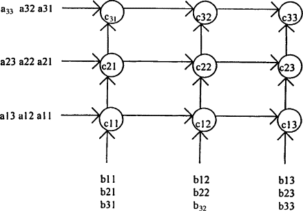
Systolic arrays are highly efficient hardware architectures designed for performing repetitive numerical computations, particularly matrix multiplication and convolution, in a structured and pipelined manner. The term “systolic” refers to the rhythmic, pulse-like propagation of data through a grid of processing elements (PEs), similar to the heartbeat. This design enables massive parallelism while minimizing external memory access, making it highly suitable for applications in linear algebra, deep learning accelerators, and signal processing.
The key principle behind systolic arrays is that each PE performs a simple computation—typically a multiply-accumulate (MAC)—and forwards its inputs to neighboring PEs. This allows each element of the input matrices to be reused across multiple PEs, reducing memory bandwidth requirements. Additionally, the regular, local communication between PEs makes the array highly scalable and amenable to pipelining.
Mathematical Background and Efficiency
Consider the multiplication of two matrices, (A \in \mathbb{R}^{N \times M}) and (B \in \mathbb{R}^{M \times K}), producing a matrix (C \in \mathbb{R}^{N \times K}):
\[ C_{ij} = \sum_{k=0}^{M-1} A_{ik} \cdot B_{kj}, \quad 0 \le i < N, \ 0 \le j < K \]
A naive implementation would require fetching elements of (A) and (B) from memory for each multiplication, leading to high memory bandwidth and latency. Systolic arrays mitigate this by streaming the elements of (A) across rows and elements of (B) across columns. Each PE receives one element from (A) and one from (B), performs a multiplication, adds it to an internal accumulator, and forwards the operands to neighboring PEs.
Mathematically, the computation within a PE can be expressed as:
\[ c_{ij}^{(k)} = c_{ij}^{(k-1)} + a_{ik} \cdot b_{kj} \]
where (c_{ij}^{(k)}) is the partial sum after processing the (k)-th element of the summation. By distributing the summation across a 2D grid of PEs and pipelining the inputs, the systolic array achieves:
-
Parallelism: Each PE operates concurrently, producing one partial sum per clock cycle.
-
Data Locality: Operands move only to immediate neighbors, minimizing global memory access.
-
Pipelining: Once the array is filled, one output per PE per clock cycle can be produced continuously.
This structure allows for high throughput and energy efficiency, especially for large matrices.
GEMM Implementation
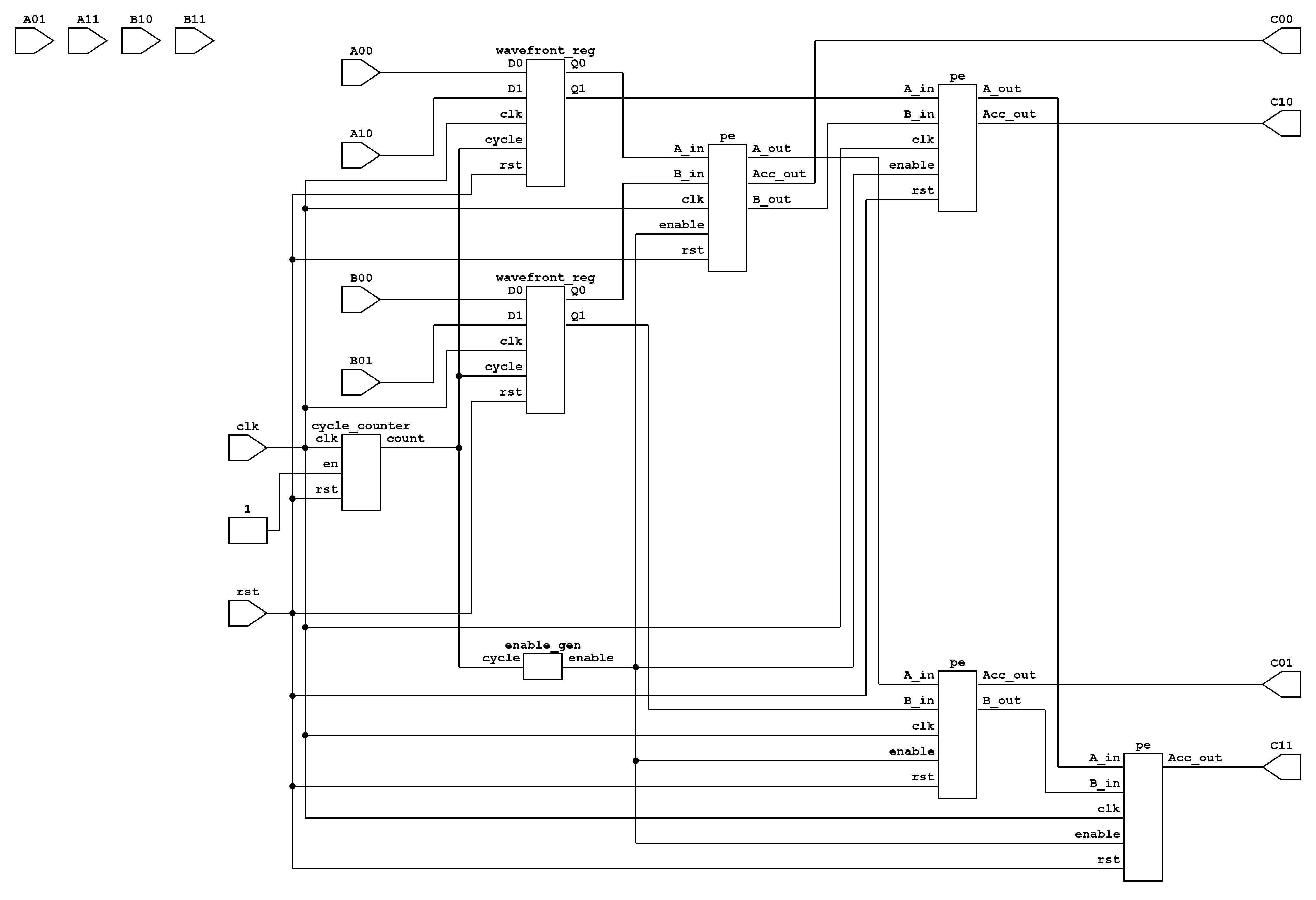
The general matrix multiplication (GEMM) is implemented using a 2D grid of PEs. Each PE maintains a local accumulator, performs a multiply-accumulate operation, and forwards the operands to the next PE in its row or column. The top-level module organizes the PEs to multiply an (N \times M) matrix (A) with an (M \times K) matrix (B) to produce (C \in \mathbb{R}^{N \times K}).
Processing Element (PE)
Each PE implements a multiply-accumulate operation:
module pe(
    input clk,
    input rst,
    input [7:0] a_in,
    input [7:0] b_in,
    output reg [7:0] a_out,
    output reg [7:0] b_out,
    output reg [15:0] c_out
);
    reg [15:0] acc;

    always @(posedge clk or posedge rst) begin
        if (rst) begin
            a_out <= 0;
            b_out <= 0;
            c_out <= 0;
            acc   <= 0;
        end else begin
            a_out <= a_in;
            b_out <= b_in;
            acc   <= acc + a_in * b_in;
            c_out <= acc;
        end
    end
endmodule
The PE is fully pipelined: ‘a_in’ and ‘b_in’ are forwarded to the next PE while the internal accumulator updates the partial sum. This local accumulation avoids repeated memory accesses for intermediate sums.
Top-Level Systolic Array
The PEs are arranged in an (N \times K) grid, enabling the computation of all (C_{ij}) elements in parallel. Input streams are delayed appropriately using registers to align operands across the array. The top-level module can be parameterized for any matrix dimensions (N), (M), and (K):
module top #(
    parameter N = 4,
    parameter M = 4,
    parameter K = 4
)(
    input clk,
    input rst,
    input [7:0] a_in [0:N-1][0:M-1],
    input [7:0] b_in [0:M-1][0:K-1],
    output [15:0] c_out [0:N-1][0:K-1]
);
    // Instantiate PEs in an NxK grid
    // Forward a_in along rows, b_in along columns
    // Each PE computes partial sums
endmodule
The testbench only sequences the input matrices into the array and observes the output. Because the computation is fully pipelined, the testbench logic is minimal and does not introduce additional complexity. Its primary function is to verify correctness for different input sizes.
This GEMM implementation using systolic arrays achieves high throughput and energy efficiency by exploiting parallelism, pipelining, and local communication. The parameterized design allows scaling to arbitrary (N \times M \times K) matrices, making it suitable for hardware accelerators where matrix multiplication dominates computation time.
Convolutional Layer Implementation (Conv2D)
A 2D convolution operation computes a weighted sum over a sliding window of the input image. Mathematically, for an input image (I \in \mathbb{R}^{N \times N}) and a kernel (K \in \mathbb{R}^{K \times K}):
\[ O_{i,j} = \sum_{m=0}^{K-1} \sum_{n=0}^{K-1} I_{i+m,j+n} \cdot K_{m,n}, \quad 0 \le i,j < N-K+1 \]
Two common convolution modes are valid (no padding, output smaller than input) and same (zero-padding, output same size as input).
Systolic Array Mapping and Inner Modules
 {width=“100%”}
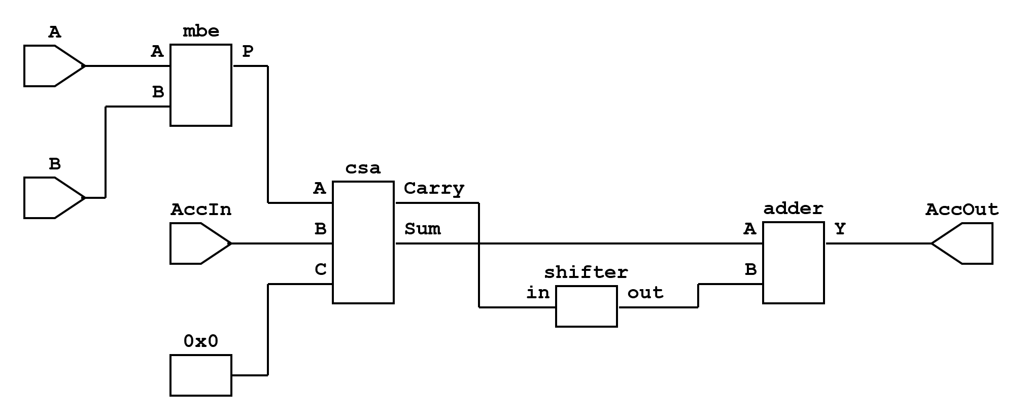
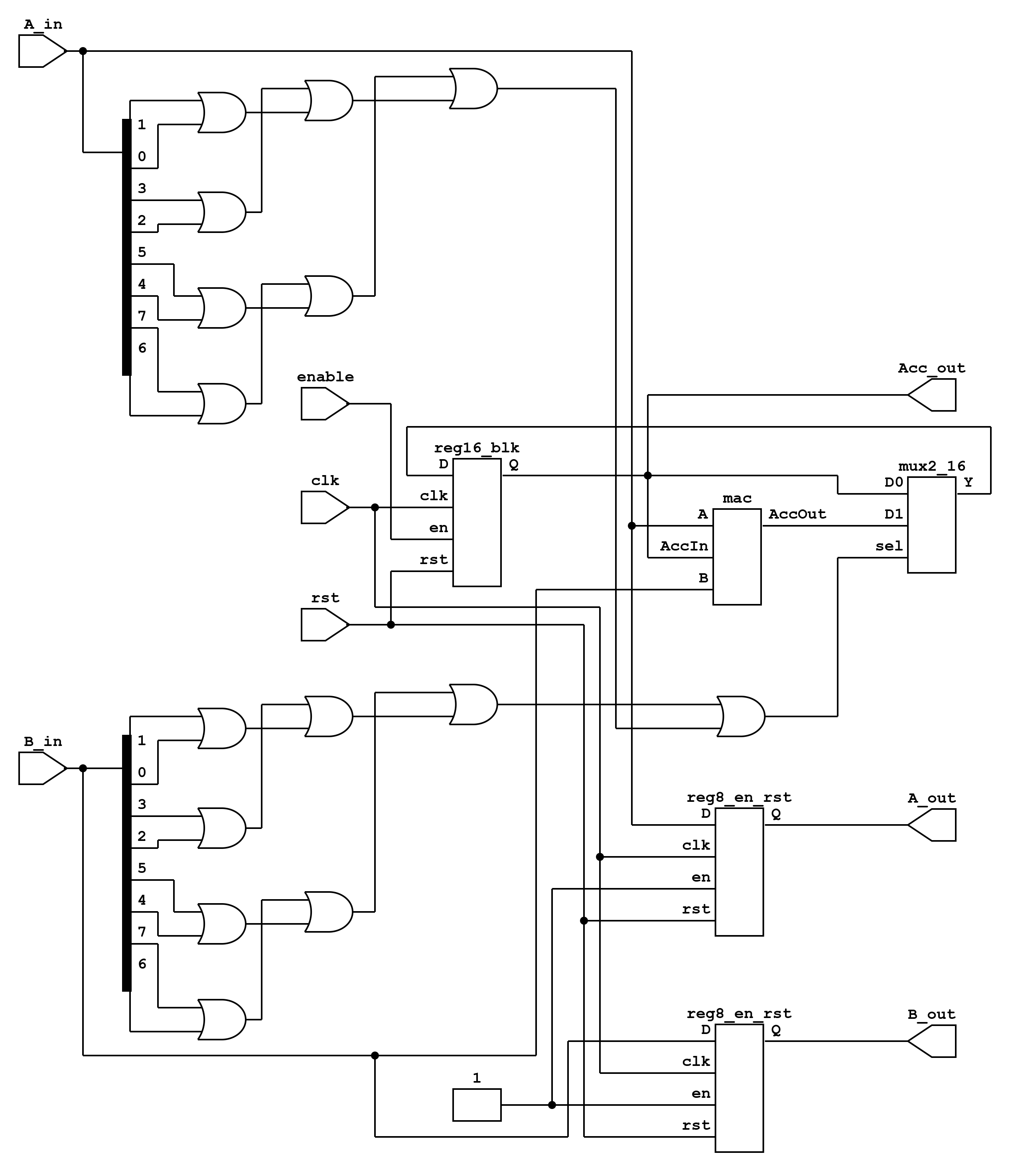
The 3x3 convolution is mapped to a systolic structure composed of 9 processing elements (PEs), each being a multiply-accumulate (MAC) unit. Every PE takes one pixel and one kernel weight, computes a product, and contributes it to the convolution sum. These 9 products are then aggregated through a tree of carry-save adders (CSAs) to produce the final convolution output.
-
Processing Element (PE): Each PE is realized as a MAC unit that accepts an 8-bit signed pixel ((A)), an 8-bit signed kernel coefficient ((B)), and a 16-bit accumulator input. Internally, it uses:
-
A Booth multiplier for signed 8(\times)
<!-- -->{=html}8 multiplication, producing a 16-bit product. -
A carry-save adder (CSA) to add the product, the accumulator input, and a zero.
-
A final carry-propagate adder that combines the CSA’s sum and shifted carry outputs, generating the accumulated result.
This design minimizes critical path delay while allowing pipelining of MAC results.
-
-
CSA Tree for Accumulation: Since 9 MAC units operate in parallel, their outputs must be combined efficiently. A three-level CSA tree is employed: $$\begin{aligned} (P_0,P_1,P_2) &\rightarrow (s_0, c_0) \ (P_3,P_4,P_5) &\rightarrow (s_1, c_1) \ (P_6,P_7,P_8) &\rightarrow (s_2, c_2)
\end{aligned}$$ The final result is computed as: \[ Out = (s_0+s_1+s_2) + ((c_0+c_1+c_2) \ll 1) \] This reduces delay compared to a single 9-input adder.
-
Pipeline Registers:
-
Stage0: Holds sampled 16-bit pixel values (‘px16_s0’) from the input image.
-
Stage1: Truncates pixel and kernel values to 8 bits for MACs (‘px8_s1’, ‘ker8_s1’).
-
Stage2: Registers MAC outputs (‘prod_s2’) before feeding them to the CSA tree.
-
Pipeline Flow and Data Alignment
The convolution pipeline operates as follows:
-
Sampling Window: The FSM scans the input image, extracting a 3x3 window for each output pixel. For same convolution, padding is applied by inserting zeros where indices go out of bounds.
-
Kernel Flipping: The kernel is flipped prior to computation to satisfy the convolution definition.
-
Stage Propagation:
-
Pixels from ‘px16_s0’ are truncated to 8-bit values and forwarded to MAC units in Stage1.
-
MAC outputs (‘prod_wire’) are registered into ‘prod_s2’ in Stage2 to align with the CSA pipeline.
-
-
Valid Alignment: A 3-bit shift register (‘valid_pipe’) tracks the propagation of valid data through the stages. When ‘valid_pipe\[2\]’ is high, the output corresponds to a fully computed convolution value.
-
Output Counters: ‘out_row_cnt’ and ‘out_col_cnt’ track the spatial position of the output pixel. These counters advance only when an output is emitted.
Verilog Implementation Overview
The design instantiates:
-
9 MAC units, each forming a PE.
-
3 CSAs, reducing 9 partial products into final sum.
-
FSM + pipeline control logic, ensuring continuous throughput, flush handling, and SAME/VALID mode support.
Key Architectural Features
-
PE-level parallelism: All 9 multiplications happen simultaneously.
-
MAC architecture: Booth multiplier + CSA + final adder reduces critical path delay.
-
CSA accumulation: Parallel reduction tree for 9 products avoids long adder chains.
-
Stage-by-stage pipelining: Continuous data flow, one output per cycle after pipeline fill.
-
Flush support: Pipeline always propagates valid signals until the last output is produced.
-
Flexible convolution modes: SAME with zero-padding, or VALID without padding.
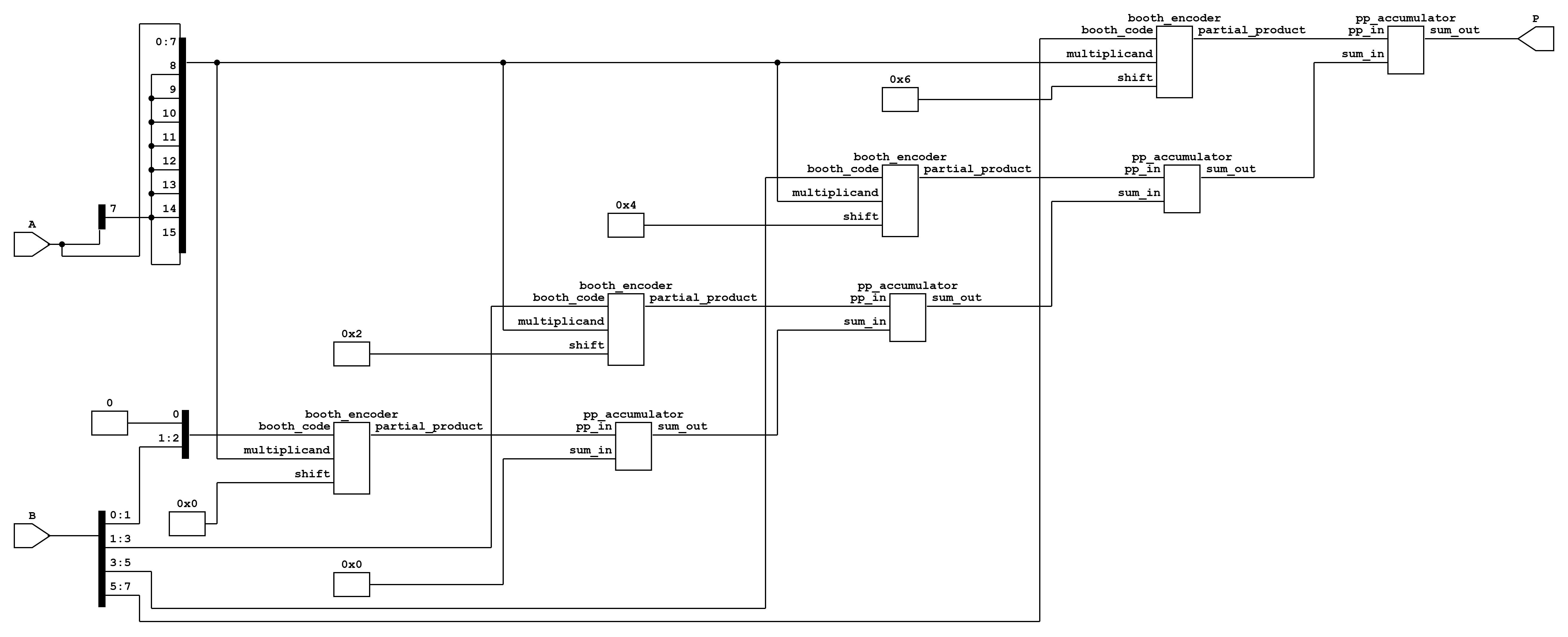
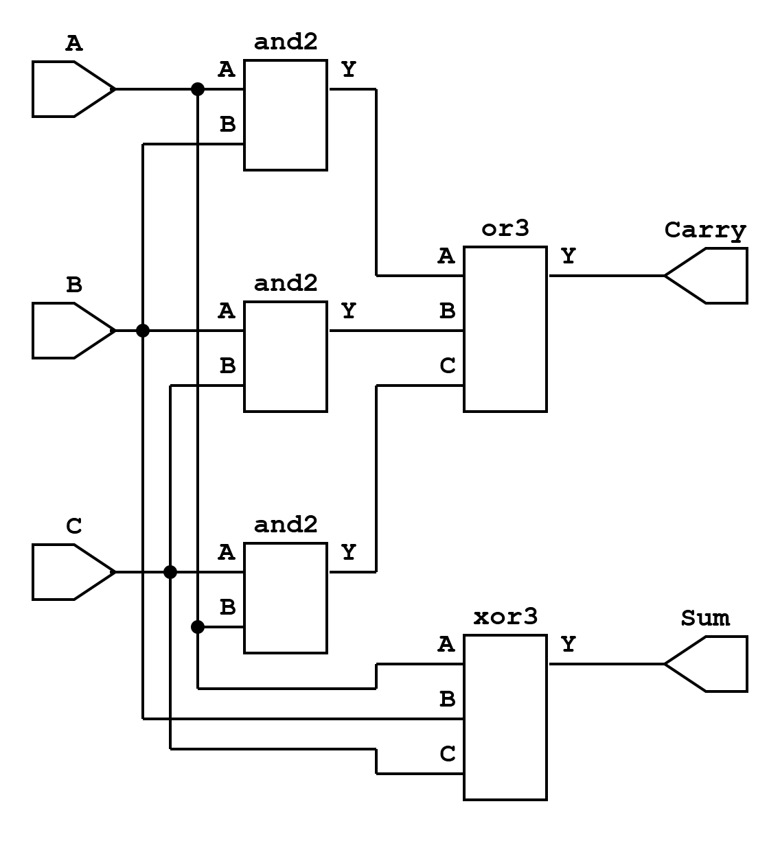
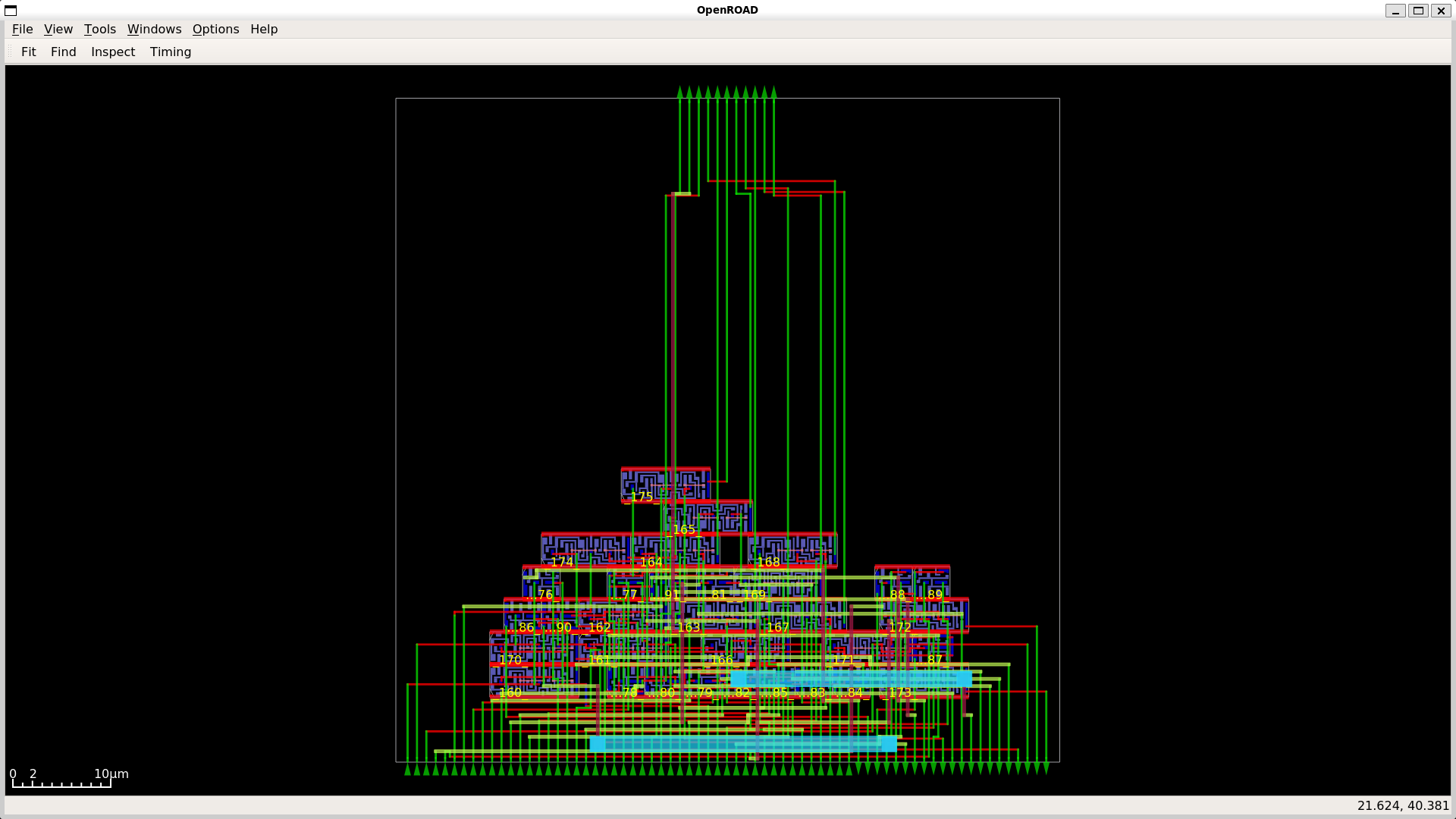
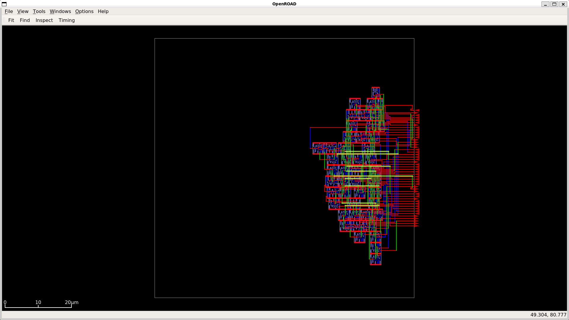
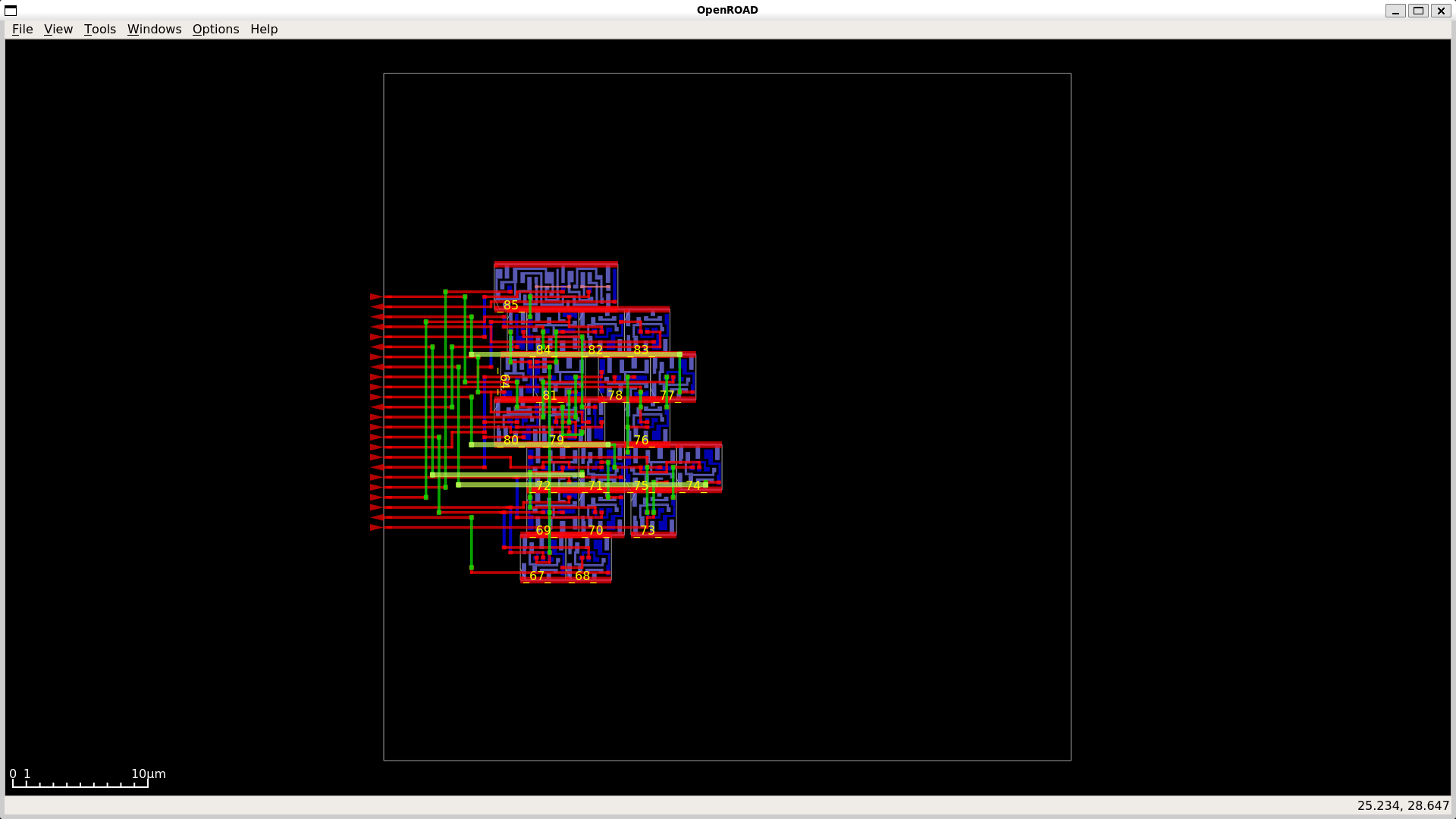
Yosys Netlists of Modules
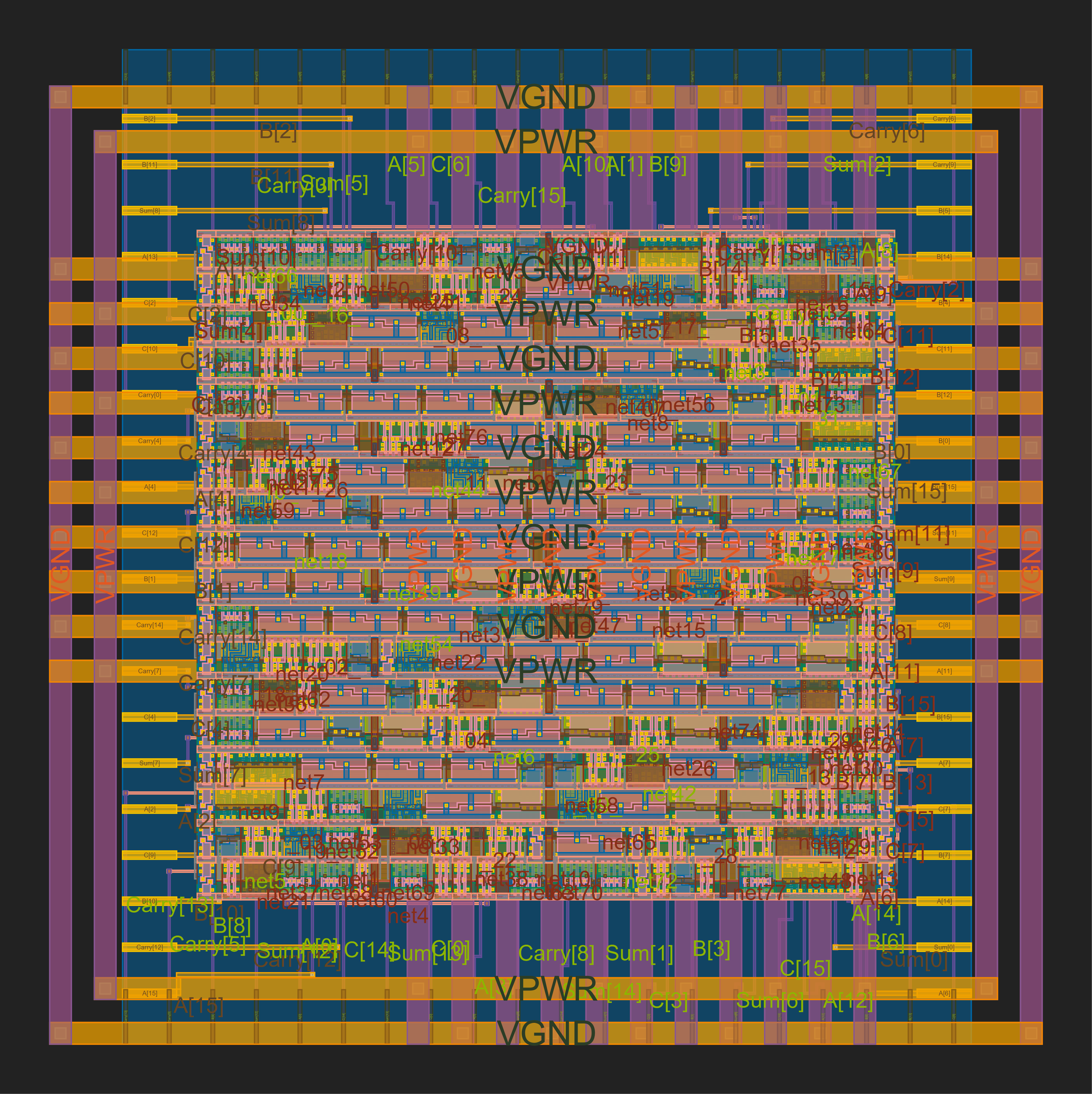
To validate the register–transfer level design and visualize the datapath structure, Yosys was used to generate netlists for the major building blocks. These netlists illustrate how arithmetic primitives and processing elements are interconnected within the systolic arrangement.
 {width=“100%”}
 {width=“50%”}
 {width=“50%”}
 {width=“50%”}
 {width=“50%”}
Comparison of MAC Unit Architectures
In high-throughput accelerators such as systolic arrays for GEMM and Conv2D, the performance of individual MAC units cannot be considered in isolation. When multiple MAC units are paired or arranged in a 2D array, additional waiting cycles occur due to pipeline alignment, data propagation, and carry-save accumulation. Consequently, the latency of a combined MAC pair or array is always higher than the latency of a single MAC unit, while throughput may be limited by interconnect delays and output readiness. This subsection analyzes both adder and multiplier architectures to highlight these effects.
8-bit Signed Adders
| Metric | CSA | Kogge–Stone | RCA |
|---|---|---|---|
| Core Area ((\mu)m²) | 2,522 | 3,689 | 1,126 |
| Die Area ((\mu)m²) | 4,604 | 6,093 | 2,572 |
| Utilization (%) | 54.79 | 60.54 | 43.79 |
| Flip-Flops | 0 | 0 | 0 |
| Total Cells | 64 | 110 | 34 |
| Combinational Cells | 64 | 110 | 34 |
| Clock Period (ns) | 10.00 | 10.00 | 10.00 |
| Critical Path (ns) | 5.07 | 6.21 | 7.14 |
| Fmax (MHz) | 197.24 | 161.03 | 140.06 |
| Total Power (mW) | 0.0834 | 0.0957 | 0.0326 |
| Energy per Cycle (pJ) | 0.834 | 0.957 | 0.326 |
| Latency (ns) | 5.07 | 6.21 | 7.14 |
| Throughput (ops/s) | 197,238,700 | 161,030,600 | 140,056,000 |
| Energy per Operation (pJ) | 422.84 | 594.30 | 232.76 |
| Power Efficiency (ops/s per mW) | 2,364,972,000 | 1,682,660,000 | 4,296,197,000 |
| Area Efficiency (ops/s per (\mu)m²) | 42,839.65 | 26,429.79 | 54,459.20 |
Observations:
-
CSA achieves the shortest critical path (5.07 ns) and highest Fmax (197 MHz) due to parallel partial sum computation.
-
RCA is the most compact and energy-efficient, but its simple ripple structure results in the slowest performance.
-
Kogge–Stone has high speed theoretically, but wire-driven delays and dense prefix logic increase area and practical delay.
8-bit Signed Multipliers
| Metric | MBE | Booth | Baugh–Wooley |
|---|---|---|---|
| Core Area ((\mu)m²) | 9,594 | 14,369 | 11,911 |
| Die Area ((\mu)m²) | 13,094 | 18,687 | 15,827 |
| Utilization (%) | 73.27 | 76.89 | 75.26 |
| Flip-Flops | 0 | 0 | 0 |
| Total Cells | 294 | 470 | 374 |
| Combinational Cells | 294 | 470 | 374 |
| Clock Period (ns) | 10.00 | 10.00 | 10.00 |
| Critical Path (ns) | 8.84 | 12.50 | 8.63 |
| Fmax (MHz) | 113.12 | 80.00 | 115.87 |
| Total Power (mW) | 0.379 | 0.701 | 0.448 |
| Energy per Cycle (pJ) | 3.79 | 7.01 | 4.48 |
| Latency (ns) | 8.84 | 12.50 | 8.63 |
| Throughput (ops/s) | 113,122,200 | 80,000,000 | 115,874,900 |
| Energy per Operation (pJ) | 3,350.36 | 8,762.50 | 3,866.24 |
| Power Efficiency (ops/s per mW) | 298,475,400 | 114,122,700 | 258,649,200 |
| Area Efficiency (ops/s per (\mu)m²) | 8,639.16 | 4,281.08 | 7,321.29 |
Observations:
-
Baugh–Wooley achieves the shortest critical path (8.63 ns) and highest Fmax (115.9 MHz) due to its regular array layout.
-
Booth multiplier (Radix-2) suffers from high latency (12.5 ns) and power consumption (0.701 mW) because of additional partial product handling.
-
MBE provides the best energy efficiency and balanced area utilization, making it optimal for paired MAC deployments.
Summary of MAC Unit Efficiency
| Category | Adders Best | Multipliers Best |
|---|---|---|
| Speed / Fmax | CSA | Baugh–Wooley / MBE |
| Power | RCA | MBE |
| Area | RCA | MBE |
| Overall Efficiency | RCA (compact, efficient) | MBE (balanced) |
: Overall MAC Component Efficiency Summary
As seen in the previous section, we have selected the CSA and MBE as the final adder–multiplier pair for our design. CSA provides significantly better speed with only a modest increase in area, while MBE offers a balanced trade-off between speed, power, and area, making the combination optimal for overall MAC efficiency
Key Insight:
While these tables reflect the isolated performance of individual adders and multipliers, the effective latency of a MAC array in GEMM or Conv2D accelerators is higher due to pipeline propagation and waiting cycles. Similarly, throughput is influenced by data alignment and CSA accumulation stages, highlighting that array-level performance always differs from single-unit metrics.
Timing Estimate (MODEL_ARCH_8)
Assumptions. The following simplifying assumptions are made for estimating the latency of one forward inference:
-
The systolic convolution engine computes one convolution output (one spatial location (\times) one output channel) per clock cycle in steady state.
-
A small fixed overhead of approximately (3) cycles per kernel is incurred (kernel flip and pipeline flush).
-
Elementwise residual adds and global pooling reductions are implemented as (1) cycle per arithmetic operation.
-
The fully connected (Dense) layer is implemented with one multiply–accumulate per cycle.
-
No additional stalls are assumed from memory bandwidth or control logic.
-
Clock frequency is treated as a variable ((f)), and estimates are shown for (50, 100, 200,) and (250,\text{MHz}).
Output counts per layer.
\[ \begin{aligned} \text{conv2d (32(\times)32(\times)28)} & : 32 \cdot 32 \cdot 28 = 28{,}672 \ \text{conv2d_1 (32(\times)32(\times)28)} & : 28{,}672 \ \text{conv2d_2 (32(\times)32(\times)28)} & : 28{,}672 \ \text{conv2d_3 (16(\times)16(\times)56)} & : 16 \cdot 16 \cdot 56 = 14{,}336 \ \text{conv2d_4 (16(\times)16(\times)56)} & : 14{,}336 \ \text{conv2d_5 (16(\times)16(\times)56)} & : 14{,}336 \end{aligned} \]
\[ \text{Total convolution outputs} = 28{,}672 \times 3 + 14{,}336 \times 3 = 129{,}024 \]
Cycle accounting.
\[ \begin{aligned} \text{Base convolution cycles} &= 129{,}024 \ \text{Per-kernel overhead} &= 252 \times 3 = 756 \ \text{Residual adds} &= (32 \cdot 32 \cdot 28) + (16 \cdot 16 \cdot 56) \ &= 28{,}672 + 14{,}336 = 43{,}008 \ \text{Global average pooling} &= 56 \cdot 63 = 3{,}528 \ \text{Dense (56(\to)10)} &= 560 \end{aligned} \]
\[ \text{Total cycles} = 129{,}024 + 756 + 43{,}008 + 3{,}528 + 560 = 176{,}876 \]
Wall-clock latency.
Latency is given by \[ T = \frac{\text{cycles}}{f}. \]
| Clock Frequency (f) | Period | Latency (T) |
|---|---|---|
| (50,\text{MHz}) | (20,\text{ns}) | (176{,}876 / 50{\times}10^{6} \approx 3.54,\text{ms}) |
| (100,\text{MHz}) | (10,\text{ns}) | (176{,}876 / 100{\times}10^{6} \approx 1.77,\text{ms}) |
| (200,\text{MHz}) | (5,\text{ns}) | (176{,}876 / 200{\times}10^{6} \approx 0.88,\text{ms}) |
| (250,\text{MHz}) | (4,\text{ns}) | (176{,}876 / 250{\times}10^{6} \approx 0.71,\text{ms}) |
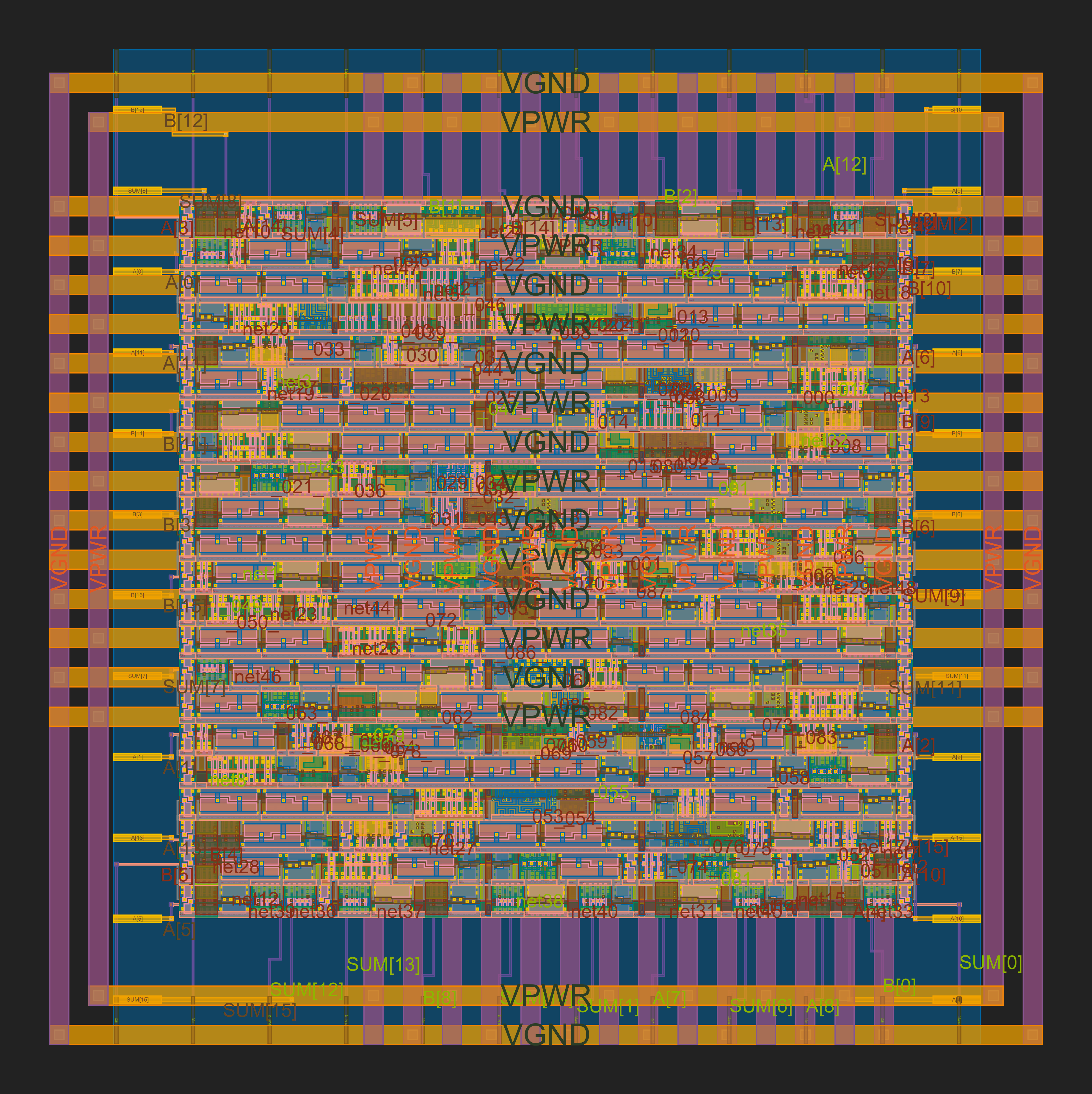
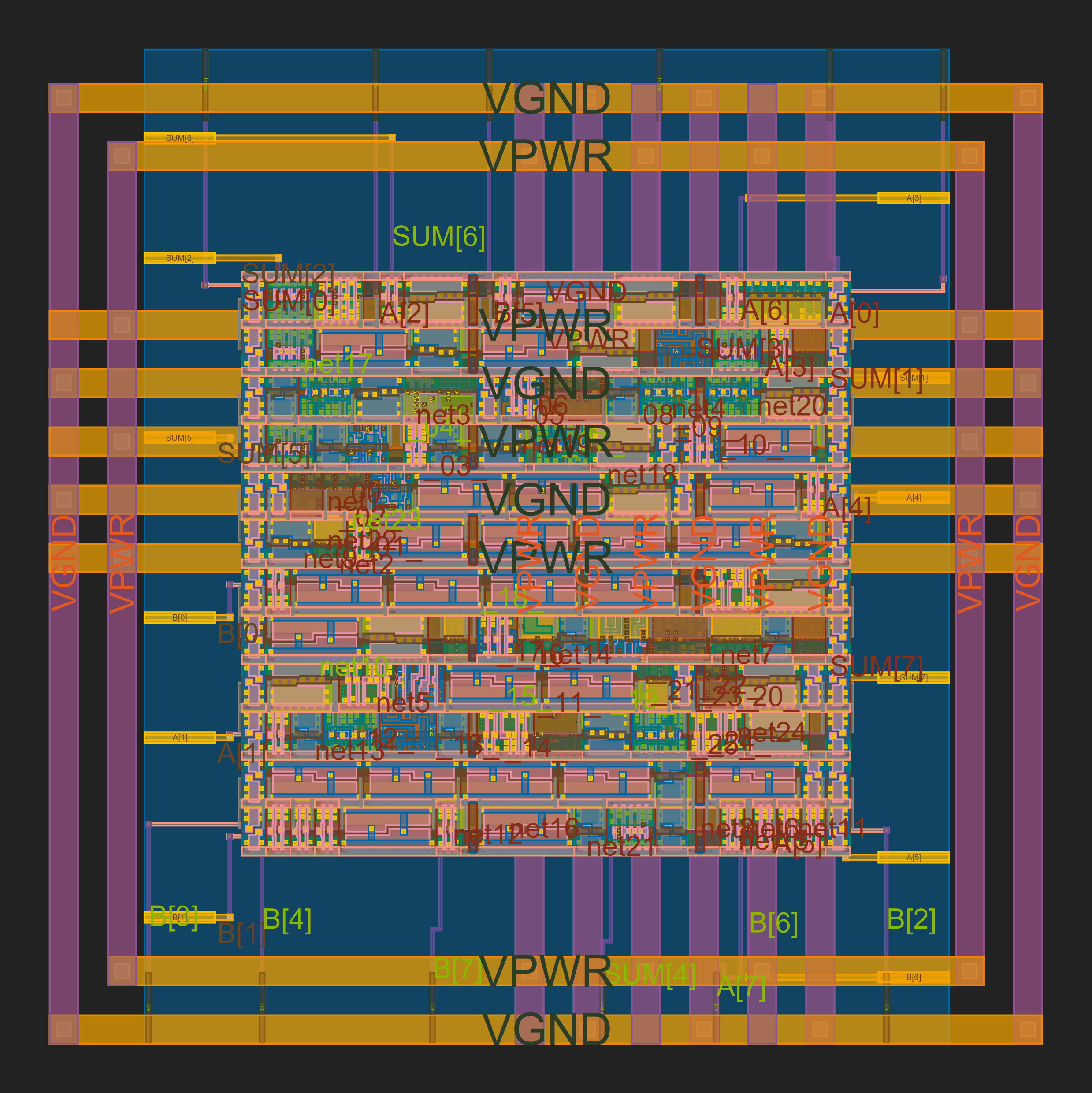
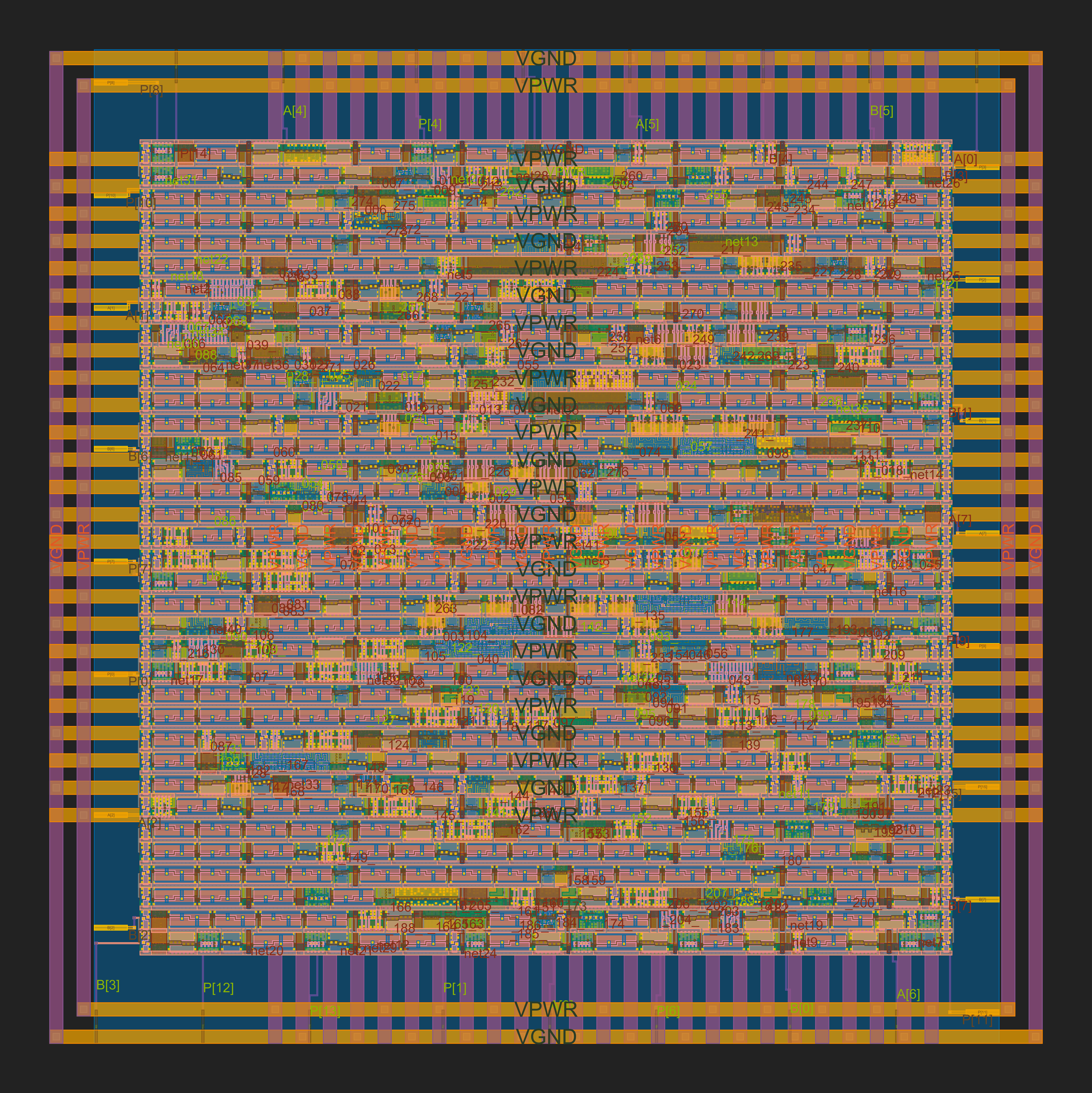
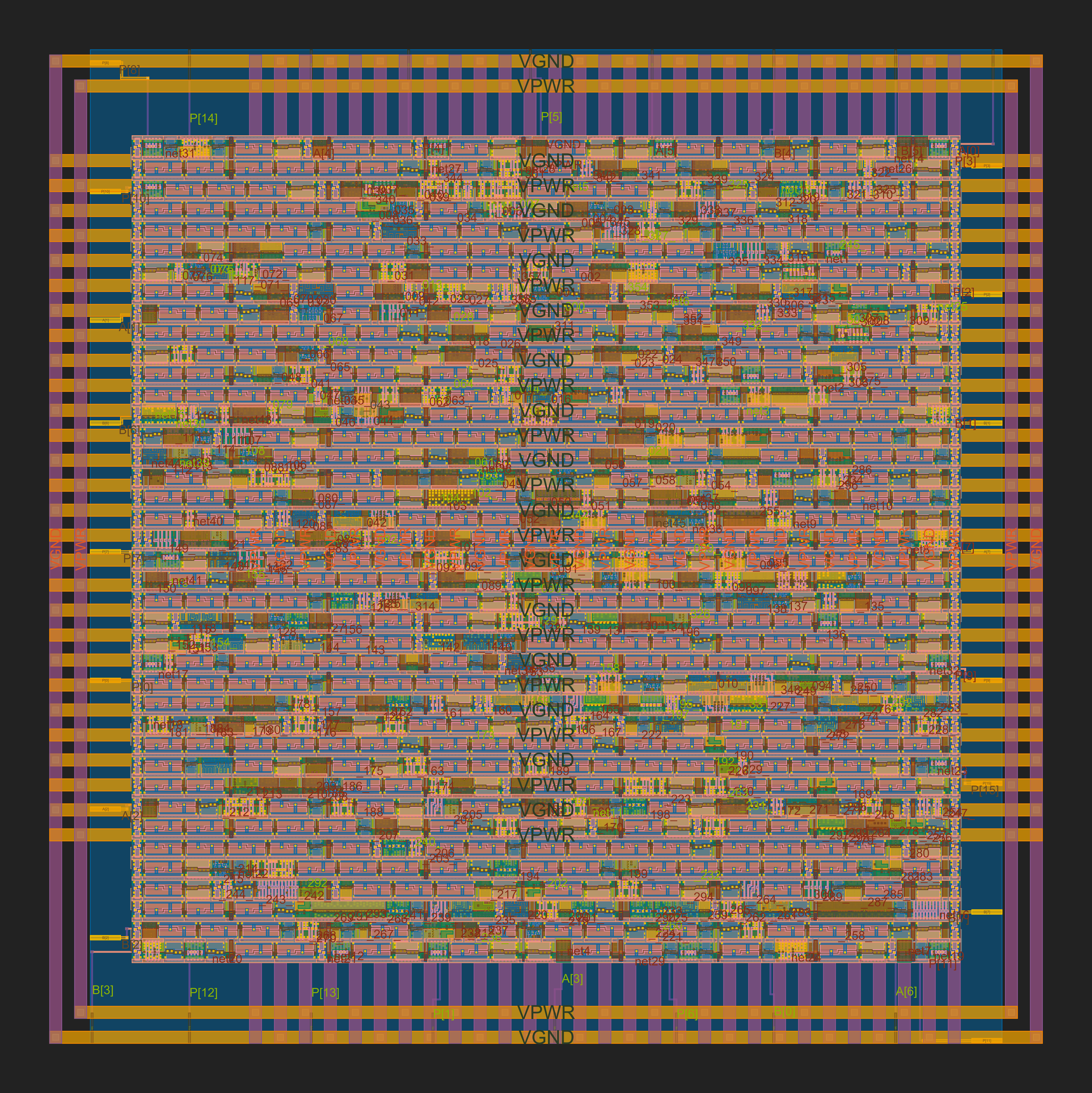
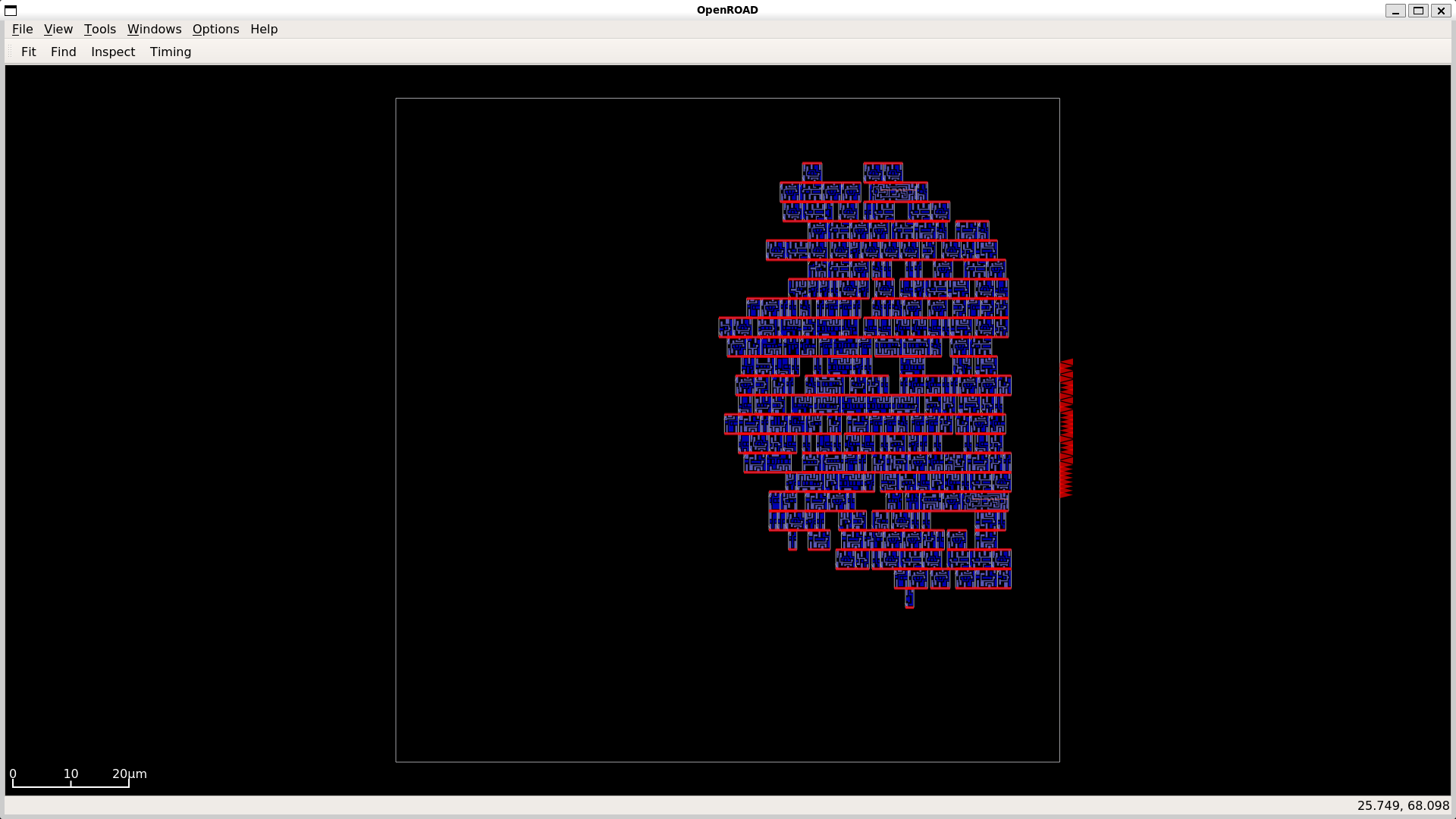
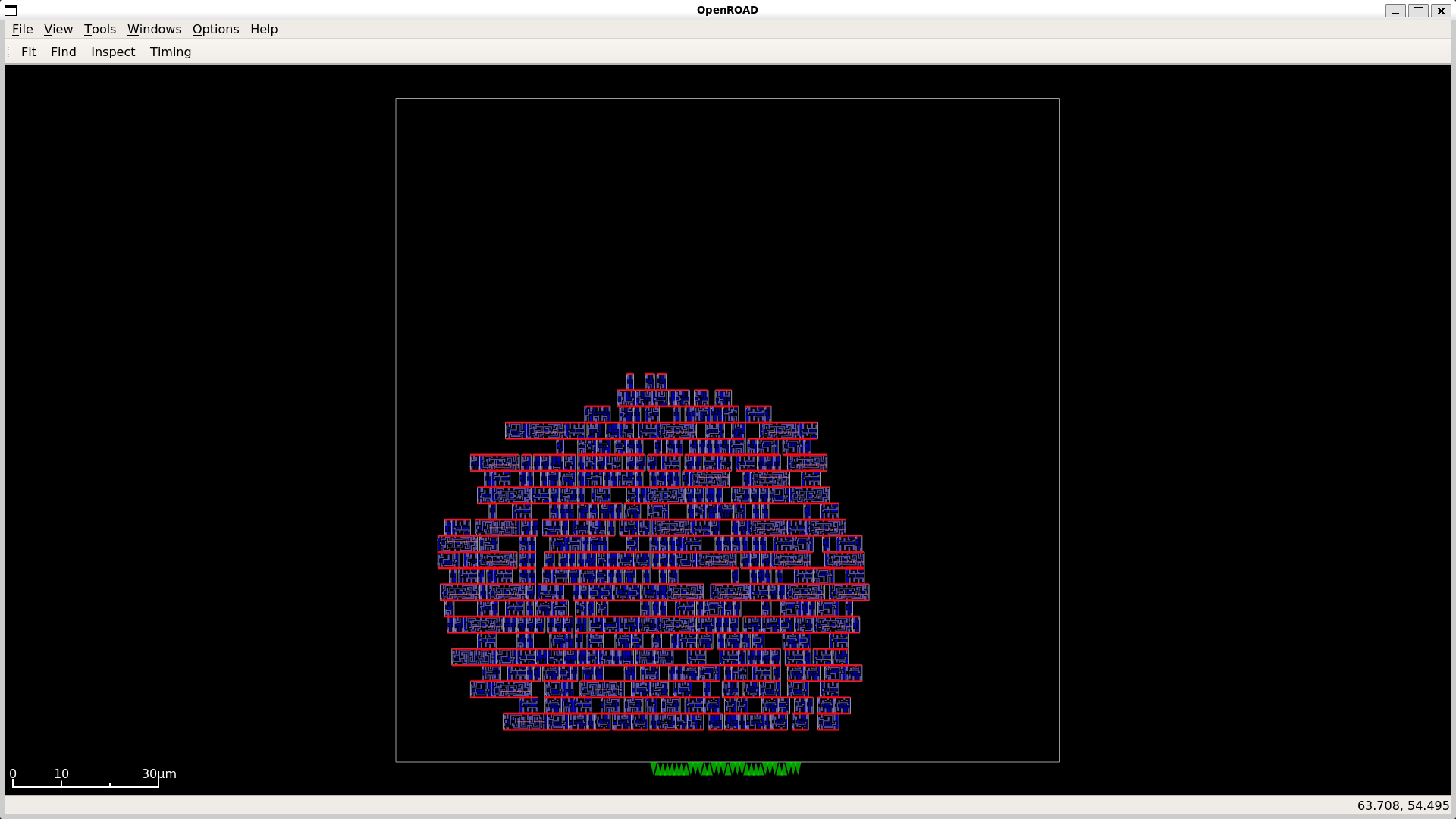
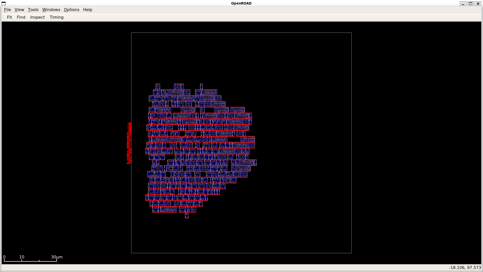
GDS and Layout Visualizations for Adders and Multipliers
Adder Visualizations
 |
 |
 |
 |
 |
 |
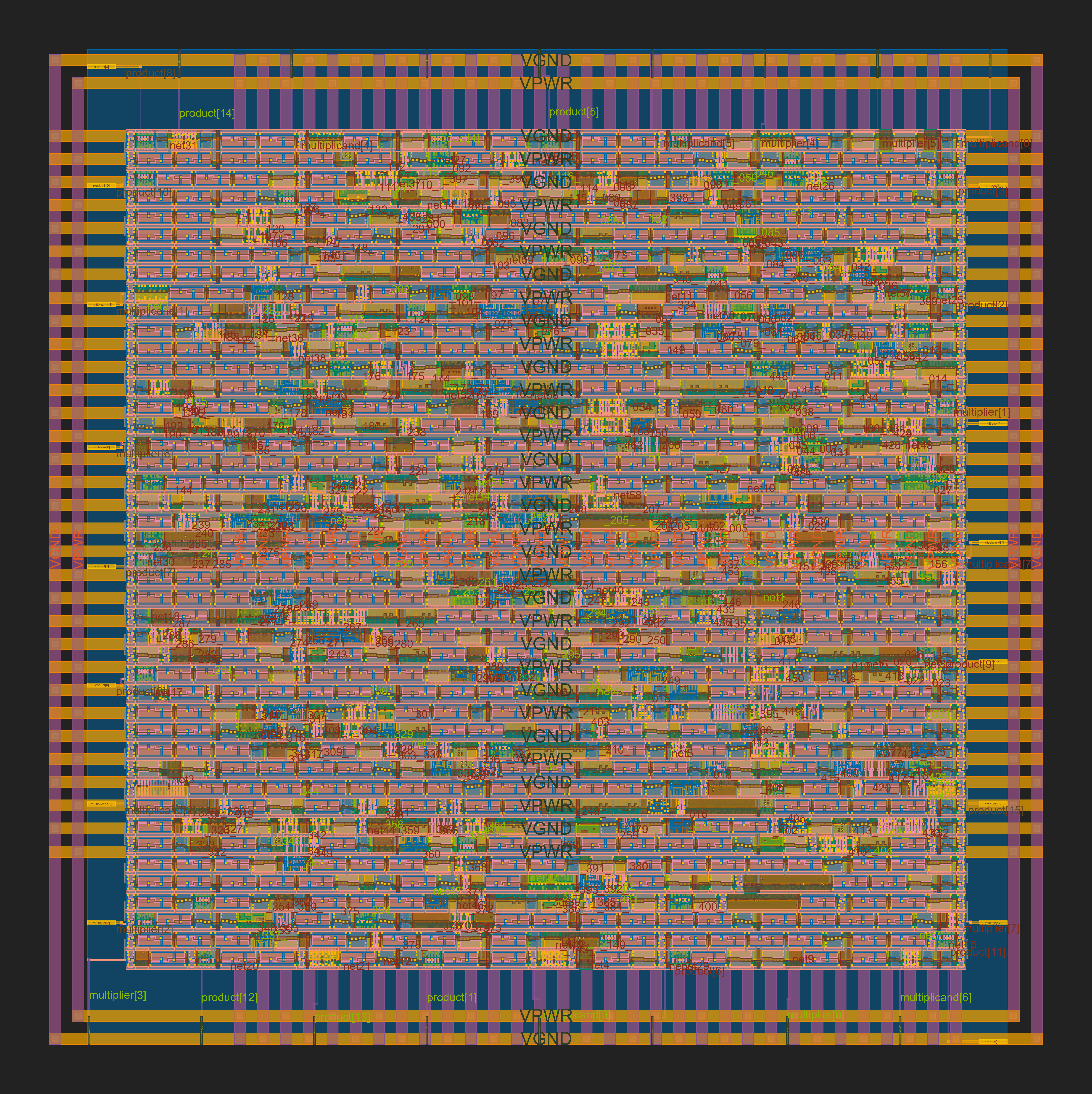
Multiplier Visualizations
 |
 |
 |
 |
 |
 |
Note on Environment and Verification Setup
All synthesis and verification experiments were carried out in a consistent flow, using the same TCL scripts and Yosys synthesis scripts. This uniform environment ensures that results are directly comparable without any tool-induced bias. Each RTL module was verified against its dedicated testbench, and post-synthesis reports confirmed that all designs met the specified timing requirements.
For technology mapping, only the SkyWater 130 nm (Sky130) open-source PDK was used. This PDK is provided through a collaboration between Google and SkyWater Technology, enabling open-source access to a fully characterized standard-cell library. The Sky130 platform allows digital design, synthesis, place-and-route, and verification flows to be tested on a real CMOS technology node.
Specifically, the standard-cell library used for synthesis was:
sky130_fd_sc_hs__tt_025C_1v80.lib
Breaking down the naming convention:
-
sky130 – Refers to the SkyWater 130 nm technology node.
-
fd – Denotes the "foundry" designation.
-
sc – Standard-cell library.
-
hs – High-speed (HS) flavor of the library, optimized for performance at the cost of area and power.
-
tt – Typical process corner (typical NMOS, typical PMOS), representing nominal manufacturing conditions.
-
025C – Temperature corner at (25^{\circ})C, i.e., room temperature.
-
1v80 – Operating supply voltage of 1.80 V.
sky130_fd_sc_hs__tt_025C_1v80.lib represents a standard-cell library
characterized for the Sky130 process, using the high-speed cell set,
under typical conditions at 25(^{\circ})C and 1.8 V supply. This ensures
that synthesis, timing analysis, and verification are carried out on a
realistic and industry-compatible open-source technology.