Ping-Pong Wrapper — Tiled GEMM
GEMM Wrapper — Memory Hierarchy Layer
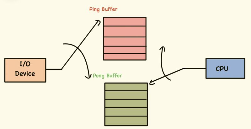
A memory-hierarchy wrapper around the existing gemm systolic array. Adds ping-pong
SRAM double-buffering for operands, a C-tile accumulation buffer, and a sequencer FSM —
turning the bare streaming datapath into a self-timed tile engine.
The five new modules are:
| Module | Role |
|---|---|
sram_bank |
Primitive single-port synchronous SRAM |
ping_pong_buf |
Double-buffered operand SRAM (A or B) |
output_buf |
C-tile staging and partial-sum accumulation |
gemm_ctrl |
Sequencer FSM — all control signals |
gemm_wrapper |
Top-level integration |
gemm, pe, mac, and line_buffer are unchanged.
The Problem Being Solved
The bare gemm module is a pure streaming datapath. It has no memory. Every cycle of
every tile, the caller must present a full column-slice of A and a full row-slice of B
on a_in and b_in. The caller also has to track done, align clr_in, enforce the
minimum inter-tile gap, and guarantee back-pressure-free delivery. At scale this is
impossible to meet from DRAM bandwidth alone — the array sits idle waiting for data.
The wrapper solves this by decoupling loading from computing:
- While the array computes tile i from the active SRAM bank, the host DMA fills the shadow bank with tile i+1.
- When tile i finishes, the banks swap in one cycle. The array immediately starts tile i+1 without a stall.
- The sequencer handles
clr_in,valid_in, bank-flip timing, and output capture automatically.
Math and Throughput
Tile parameters
M  = PE rows     = output rows of C
N  = PE columns  = output cols of C
K  = dot-product depth

MAC-ops per tile  = M × N × K
Pipeline timing inside gemm
DONE_DELAY = K + (M-1) + (N-1)
MIN_GAP    = (M-1) + (N-1)
T_tile     = K + MIN_GAP  =  DONE_DELAY
DONE_DELAY is the number of cycles from the first valid_in=1 until done goes high.
It has two parts:
- K cycles — the dot-product accumulation depth. Each PE needs K beats of operands.
- (M-1)+(N-1) cycles — wavefront drain. The last data beat enters PE(0,0) on RUNNING cycle K-1, but it takes (i+j) more cycles to reach PE(i,j) through the PE pass-through registers. The farthest PE is PE(M-1,N-1) at distance M+N-2 = MIN_GAP.
T_tile is the minimum legal period between consecutive tile starts. After K cycles of
valid data, the caller must leave at least MIN_GAP idle cycles before the next clr_in.
The optimal back-to-back period is exactly T_tile = K + MIN_GAP = DONE_DELAY.
Theoretical peak throughput
Peak = (M × N × K) / T_tile  MAC-ops/cycle
     = (M × N × K) / (K + (M-1) + (N-1))
For M=N=K=3: Peak = 27 / 7 ≈ 3.86 MAC-ops/cycle
PE utilisation
Each PE accumulates for K cycles out of every T_tile cycle period:
PE utilisation = K / T_tile = K / (K + M + N - 2)
For M=N=K=3: 3/7 ≈ 42.9% asymptotic.
The idle fraction (MIN_GAP/T_tile = 4/7 ≈ 57%) is the wavefront drain overhead. It shrinks as K grows relative to M+N. For a Conv2d tile (M=4, N=16, K=36): K/T_tile = 36/54 ≈ 66.7%.
Wrapper overhead
The wrapper adds 2 cycles of PRELOAD (FLIP_INIT + PRELOAD state) before each tile and 1 cycle of CAPTURE_WAIT + CAPTURE + WRITEBACK after. For long tiles (large K) this overhead is negligible. For M=N=K=3 it adds 8 cycles to the first tile latency:
First c_out_valid latency from start = FLIP_INIT(1) + PRELOAD(1) + DONE_DELAY(7) +
                                       CAPTURE_WAIT(1) + CAPTURE(1) + WRITEBACK(1)
                                     = 12 cycles minimum
Measured: 15 cycles (includes 2 extra cycles for PRELOAD_A and the registered
out_we delay stage).
Architecture
                        ┌─────────────────────────────────────────────────┐
                        │               gemm_wrapper                      │
                        │                                                 │
  a_wr_en/addr/data ───►│  ┌─────────────────┐   rd_en, rd_addr          │
                        │  │  ping_pong_buf  │───────────────────────►   │
  b_wr_en/addr/data ───►│  │  (A banks ×2)  │  a_rd_raw[8M-1:0]         │
                        │  └─────────────────┘      │                    │
                        │                           │ (gated by rd_en)   │
                        │  ┌─────────────────┐      ▼                    │
                        │  │  ping_pong_buf  │  ┌──────────────────┐     │
                        │  │  (B banks ×2)  │─►│      gemm        │     │
                        │  └─────────────────┘  │  (unchanged)     │     │
                        │                        └────────┬─────────┘     │
                        │  ┌─────────────────┐           │ c_out_w       │
                        │  │   output_buf    │◄──────────┘               │
                        │  │  (C tile latch) │  out_we_r, out_flush_r    │
                        │  └────────┬────────┘                           │
                        │           │ c_out_data, c_out_valid             │
                        │  ┌────────┴────────┐                           │
                        │  │   gemm_ctrl     │ valid_in, clr_in          │
                        │  │   (FSM)         │─────────────────────────► │
                        │  └─────────────────┘ flip_en, rd_en, rd_addr   │
                        │      ▲                                         │
                        │   start, done                                  │
                        └─────────────────────────────────────────────────┘
Module Reference
sram_bank
Single-port synchronous SRAM. Synthesisable behavioural model — in a real tape-out this would be replaced by a foundry SRAM macro.
Parameters: DATA_WIDTH, DEPTH, ADDR_WIDTH = $clog2(DEPTH)
Ports:      clk, we, oe, addr, wdata, rdata
Read latency: 1 cycle. rdata is registered at every posedge. oe (output enable)
gates rdata to zero when low — this is the mechanism that prevents DRAIN-phase SRAM
residue from reaching the PE array.
posedge clk:
  if (we)   mem[addr] <= wdata
  if (oe)   rdata <= mem[addr]
  else      rdata <= 0
rdata is a reg, so it holds its last value. Setting oe=0 forces it to zero on the
next posedge — important for the SRAM → gemm pipeline cleanliness.
ping_pong_buf
Wraps two sram_bank instances. One bank is active (read port feeds gemm). The other
is shadow (write port receives the next tile from the host). A flip_en pulse swaps
roles on the next posedge.
Parameters: DATA_WIDTH, DEPTH
Ports:      clk, rst, flip_en, bank_sel (out),
            rd_en, rd_addr, rd_data,
            wr_en, wr_addr, wr_data
Bank assignment:
bank_sel = 0 :  bank0 = active (read)    bank1 = shadow (write)
bank_sel = 1 :  bank1 = active (read)    bank0 = shadow (write)
The write port always targets the shadow bank. The read port always targets the active bank. Simultaneous R/W to different banks is safe and expected every tile period.
          host writes           ctrl reads
              │                     │
              ▼                     ▼
         ┌─────────┐           ┌─────────┐
         │  bank1  │  shadow   │  bank0  │  active
         │ (next   │◄──wr_en   │ (curr   │──►rd_data
         │  tile)  │           │  tile)  │
         └─────────┘           └─────────┘
                    ─── flip_en ───►
         ┌─────────┐           ┌─────────┐
         │  bank1  │  active   │  bank0  │  shadow
         │ (curr   │──►rd_data │ (next   │◄──wr_en
         │  tile)  │           │  tile)  │
         └─────────┘           └─────────┘
bank_sel_d is a registered copy of bank_sel. The output mux uses bank_sel_d to
correctly align with the 1-cycle SRAM read latency — the mux selects which bank’s
rdata is presented based on which bank was active when the address was presented,
not the current cycle’s bank_sel.
output_buf
Holds one complete C tile (M×N × 32-bit) in a register file. Supports two write modes:
accumulate = 0 :  buf[i] = wr_data[i]             (overwrite — first K-partition)
accumulate = 1 :  buf[i] = buf[i] + wr_data[i]    (accumulate — subsequent K-partitions)
flush_en triggers a registered read of the entire buffer onto rd_data and asserts
c_valid for one cycle. The tricky part: we and flush_en can fire on the same cycle
(CAPTURE state). A combinational next_buf bypass solves this — rd_data reads from
the post-write value without waiting for the register to update:
wire next_buf[i] = we ? (accumulate ? buf[i]+wr_data[i] : wr_data[i]) : buf[i];
// flush_en uses next_buf, not buf, so simultaneous we+flush is correct
This is the key correctness fix: without the bypass, a simultaneous write+flush captures
the pre-write value of buf, giving stale C output.
gemm_ctrl
The sequencer FSM. Generates all control signals for gemm, the ping-pong buffers,
and output_buf. Nothing else has any autonomous control logic.
FSM states
  ┌────────┐  start  ┌───────────┐         ┌──────────┐
  │  IDLE  │────────►│ FLIP_INIT │────────►│ PRELOAD  │
  └────────┘         └───────────┘         └────┬─────┘
      ▲                                         │
      │ tile_cnt==NUM_TILES-1                   ▼
  ┌───────────┐    done  ┌──────────────┐  ┌─────────┐
  │ WRITEBACK │◄─────────│ CAPTURE_WAIT │  │ RUNNING │
  └───────────┘          └──────────────┘  └────┬────┘
       │ else                  ▲                 │ k_cnt==K-1
       ▼                       │                 ▼
  ┌──────────┐          ┌──────┴──────┐    ┌─────────┐
  │ PRELOAD  │◄─────────│   CAPTURE   │    │  DRAIN  │
  └──────────┘          └─────────────┘    └─────────┘
                                            gap_cnt==MIN_GAP-1
FLIP_INIT (1 cycle, tile-0 only): asserts flip_en. The shadow bank (loaded by the
host before start) becomes the active bank. For tiles 1+ this state is skipped —
the DRAIN flip at the end of the previous tile already did the swap.
PRELOAD (1 cycle): rd_en=1, clr_in=1. The SRAM sees rd_addr=0 with oe=1
and will output data[0] on the next cycle. clr_in=1 enters gemm’s delay lines —
it will reach PE(i,j) after i+j cycles, exactly when that PE’s first valid data arrives.
RUNNING (K cycles): valid_in=1, rd_en=1 for cycles 0..K-2, rd_en=0 on cycle
K-1 (last beat). The final rd_en=0 forces the SRAM to capture zero at the last
RUNNING posedge, so DRAIN cycle 0’s SRAM output is zero — no extra beat accumulates.
DRAIN (MIN_GAP cycles): valid_in=0. Wavefront drains. flip_en pulses on
gap_cnt=0 (first drain cycle) so the host can immediately start loading the new shadow
bank for the next tile. The host load window is T_tile = K + MIN_GAP cycles.
CAPTURE_WAIT: waits for done from gemm. done is a registered output inside
gemm, so it arrives 1-2 cycles after DRAIN ends. The FSM spins here until done=1.
CAPTURE (1 cycle): asserts out_we. This is delayed 1 cycle in the wrapper
(out_we_r) so output_buf sees the stable gemm.c_out value.
WRITEBACK (1 cycle): pulses tile_done. Returns to PRELOAD (next tile) or IDLE.
rd_addr is combinational
rd_addr is a combinational output (not registered), so the SRAM sees the address
immediately. Combined with 1-cycle SRAM latency:
PRELOAD state:   rd_addr = 0   →  SRAM output = data[0]  arrives RUNNING cy0
RUNNING cy0:     rd_addr = 1   →  data[1] arrives RUNNING cy1
RUNNING cy1:     rd_addr = 2   →  data[2] arrives RUNNING cy2
RUNNING cy2:     rd_en = 0     →  SRAM output = 0         arrives DRAIN cy0
This gives exactly K beats of valid data to PE(0,0), zero otherwise.
gemm_wrapper
Top-level. Instantiates all of the above plus gemm. No logic — just wiring and two
pipeline registers.
out_we_r / out_acc_r / out_flush_r: registered 1 cycle from ctrl outputs.
gemm.c_out is a register that latches acc[] when done=1. The ctrl asserts out_we
in CAPTURE at the same posedge that gemm.c_out latches — so output_buf would capture
the pre-latch value. Delaying the write controls by 1 cycle fixes this.
Timing Diagram (M=N=K=3, T_tile=7, MIN_GAP=4)
Cycle:  0           1     2     3     4     5     6     7     8  ...  14    15
State:  FLIP_INIT   PRE   RUN0  RUN1  RUN2  DRN0  DRN1  DRN2  DRN3  CAP   WB

rd_en:  0           1     1     1     0     0     0     0     0       0     0
rd_addr:0           0     1     2     0     0     0     0     0       0     0
SRAM:               0     d[0]  d[1]  d[2]  0     0     0     0
                          ↑     ↑     ↑     ↑
                          │     │     │     └─ SRAM captures 0 (rd_en=0 at posedge)
                          └─────┴─────┴─ K=3 valid beats to PE(0,0)

valid_in: 0         0     1     1     1     0     0     0     0
clr_in:   0         1     0     0     0     0     0     0     0
                    ↑
                    └─ clr_in enters gemm delay lines here.
                       PE(0,0) clears in PRELOAD cy (delay=0).
                       PE(1,1) clears at RUNNING cy1 (delay=2).
                       PE(2,2) clears at DRAIN cy2  (delay=4).

flip_en:  1         0     0     0     0     1     0     0     0
                    ↑                       ↑
                    └─ tile-0: shadow→active│
                                            └─ tile-0 DRAIN: swap for tile-1
                                              Host load window opens here ─────►

done (from gemm):                                                ←── rises here
                                                                        │
out_we_r: 0         0     0     0     0     0     0     0     0   0     1
c_out_valid:                                                             1
Host load window (K + MIN_GAP = 7 cycles between flip_en pulses). The host must write K words into the shadow bank within this window. At K=3, SRAM_DEPTH=8, this is comfortable at any reasonable memory bandwidth.
Ping-Pong Handshake
         Tile 0                  Tile 1                  Tile 2
         ───────                 ───────                 ───────
Bank1:   [active: data0]         [shadow: data2 loading] [active: data2]
Bank0:   [shadow: data1 loading] [active: data1]         [shadow: data3 loading]

         flip_en=1 (FLIP_INIT)   flip_en=1 (DRAIN cy0)   flip_en=1 (DRAIN cy0)
         bank_sel: 0→1           bank_sel: 1→0            bank_sel: 0→1

Host:    load bank1 before start │ load bank0 in DRAIN     │ load bank1 in DRAIN
The host detects the bank flip by watching bank_sel_a toggle. Every time it toggles,
the shadow bank is freshly available for the next tile’s data.
Challenges and Fixes
1. SRAM read latency vs clr_in alignment
Problem: clr_in is delayed i+j cycles inside gemm to reach PE(i,j). Data
arrives at PE(i,j) after (i+j) PE pass-through hops plus 1 cycle of SRAM read
latency. So data is always 1 cycle late relative to clr at every PE except PE(0,0).
PE(i,j) would accumulate one beat before clr fires, giving wrong results.
Fix: Assert clr_in in the PRELOAD state (1 cycle before RUNNING) with rd_en=0
(SRAM output = 0). When clr reaches PE(i,j) after i+j cycles, the SRAM has had i+j+1
cycles of valid output — exactly matching. Because rd_en=0 during PRELOAD, the SRAM
outputs 0 when clr fires, so the MAC clears to zero, not to some residual value.
PRELOAD:  clr_in=1, rd_en=0  →  SRAM=0  →  MAC clears to product(0,0)=0
RUNNING:  clr_in=0, rd_en=1  →  SRAM=data  →  K beats accumulate
For PE(1,1) specifically:
clr reaches PE(1,1) at  PRELOAD + 2 = RUNNING cy1
data[0] reaches PE(1,1) at RUNNING cy0 + 2 PE hops = RUNNING cy2
                                    ↑ 1 SRAM cycle already included
clr fires at cy1, data arrives cy2 → 1 cycle gap → K=3 beats (cy2, cy3, cy4). ✓
2. SRAM bleed into DRAIN — extra beat at PE(0,0)
Problem: The last RUNNING cycle (k_cnt=K-1) has rd_en=1 and the SRAM is
presenting real data. At the posedge of that cycle, the SRAM latches the last read
address and will present data[K-1] at DRAIN cy0. PE(0,0) accumulates this extra beat.
Fix: Set rd_en=0 when k_cnt==K-1 (still in RUNNING state combinationally, but
the SRAM sees oe=0 and captures 0 instead of real data). DRAIN cy0 SRAM output = 0.
PE(0,0) gets exactly K beats.
ST_RUNNING: rd_en = (k_cnt == K-1) ? 1'b0 : 1'b1;
3. output_buf simultaneous write + flush capturing stale data
Problem: out_we fires in CAPTURE state at the same posedge that gemm.c_out
latches acc[] (because gemm.done is itself registered). So output_buf would
write the pre-latch value of c_out — all zeros from the previous state.
Fix A: Delay out_we/out_acc/out_flush by 1 cycle (registered in wrapper).
By the time out_we_r fires, gemm.c_out has already settled.
Fix B: Within output_buf, when we and flush_en fire on the same cycle, use
a combinational next_buf mux to read the post-write value, not the stored register.
This handles any residual same-cycle case cleanly.
4. FLIP_INIT adds a pipeline overhead for all tiles
Problem: Early implementations re-entered FLIP_INIT on every tile, adding 1 extra idle cycle per tile to the throughput and also misaligning the clr/data timing for tiles 2+.
Fix: FLIP_INIT runs only for tile-0 (tracked by first_tile register). For tiles
1+ the FSM goes directly WRITEBACK→PRELOAD. The bank swap for tiles 1+ is handled by
DRAIN’s flip_en pulse.
nstate = (tile_cnt == NUM_TILES-1) ? ST_IDLE : ST_PRELOAD; // not ST_FLIP_INIT
5. Testbench protocol — both SRAM banks must be pre-loaded
Problem: After hard_reset, bank_sel=0 and the write port targets shadow=bank1.
We can load bank1. But tile-1 runs from bank0 (after the first DRAIN flip), which is
still zero from reset. Tile-1 produces all-zero C.
Fix: preload_both_banks task uses a dummy-flip protocol:
1. hard_reset → bank_sel=0, shadow=bank1. Load bank1 (K words).
2. Pulse start for 1 cycle → FLIP_INIT fires → bank_sel=1, shadow=bank0.
3. Load bank0 (K words) while ctrl is in PRELOAD (safe, no RUNNING yet).
4. Assert rst to cancel the dummy run → bank_sel=0, state=IDLE.
5. Both banks now contain tile data. Assert real start.
6. rd_addr must be combinational, not registered
Problem: If rd_addr is registered (as is typical for FSM outputs), there are
2 cycles from “state issues addr” to “data at SRAM output” (1 for the register, 1 for
SRAM latency). Compensating for this required 2 PRELOAD states and complex addr
sequencing that was fragile.
Fix: Make rd_addr a combinational wire assigned from always @(*). The SRAM
sees the address immediately; 1 cycle later the data is ready. The sequencing becomes:
State changes to PRELOAD → rd_addr=0 combinationally → SRAM latches → data at RUNNING cy0
One clean pipeline stage, no compensation needed.
7. CAPTURE_WAIT — gemm.done arrives later than expected
Problem: After DRAIN ends, the FSM moved directly to CAPTURE. But gemm.done is
a registered output of the valid_sr shift register inside gemm — it arrives 1 cycle
after the shift register fills. Without CAPTURE_WAIT, CAPTURE fired before done was
high and gemm.c_out had not yet latched the final accumulator values.
Fix: Add ST_CAPTURE_WAIT — a spin state that waits for done=1 before moving to
CAPTURE. Since done stays high for K cycles, CAPTURE always fires within the valid
window.
File List
| File | New / Existing |
|---|---|
sram_bank |
New |
ping_pong_buf |
New |
output_buf |
New |
gemm_ctrl |
New |
gemm_wrapper |
New |
gemm_wrapper_tb |
New |
gemm |
Existing — unchanged |
pe |
Existing — unchanged |
mac |
Existing — unchanged |
line_buffer |
Existing — unchanged |
Compile and Run
iverilog -o sim_wrapper sram_bank.v ping_pong_buf.v output_buf.v \
         line_buffer.v mac.v pe.v gemm.v \
         gemm_ctrl.v gemm_wrapper.v gemm_wrapper_tb.v && vvp sim_wrapper
Expected output: 12 PASS / 0 FAIL
Parameters
| Parameter | Default | Description |
|---|---|---|
M |
3 | PE rows / output rows of C |
N |
3 | PE columns / output cols of C |
K |
3 | Dot-product depth |
NUM_TILES |
1 | Total tiles the FSM runs before returning to IDLE |
K_PARTS |
1 | K-partitions per output tile (1 = full K at once) |
SRAM_DEPTH |
8 | Words per ping-pong bank (must be ≥ K) |
Test Coverage
| Test | What it checks |
|---|---|
| T1 | Single tile, all-ones. Basic wrapper correctness, correct latency. |
| T2 | 8 back-to-back tiles, I×I=I. Ping-pong handoff correctness, all 8 tiles pass, throughput measured. |
| T3 | K-partitioned GEMM. A(M×2K)×B(2K×N) split into 2 sub-tiles, manual accumulation matches reference. |
| T4 | Conv2d pass-through. Identity filter with channel-packed im2col input. Output = input pixels. |
| T5 | Reset mid-RUNNING. FSM returns to IDLE cleanly, correct result on restart. |